F6456 Просмотр технического описания (PDF) - Sanken Electric co.,ltd.
Номер в каталоге
Компоненты Описание
производитель
F6456 Datasheet PDF : 7 Pages
| |||
IRIS-F6454R
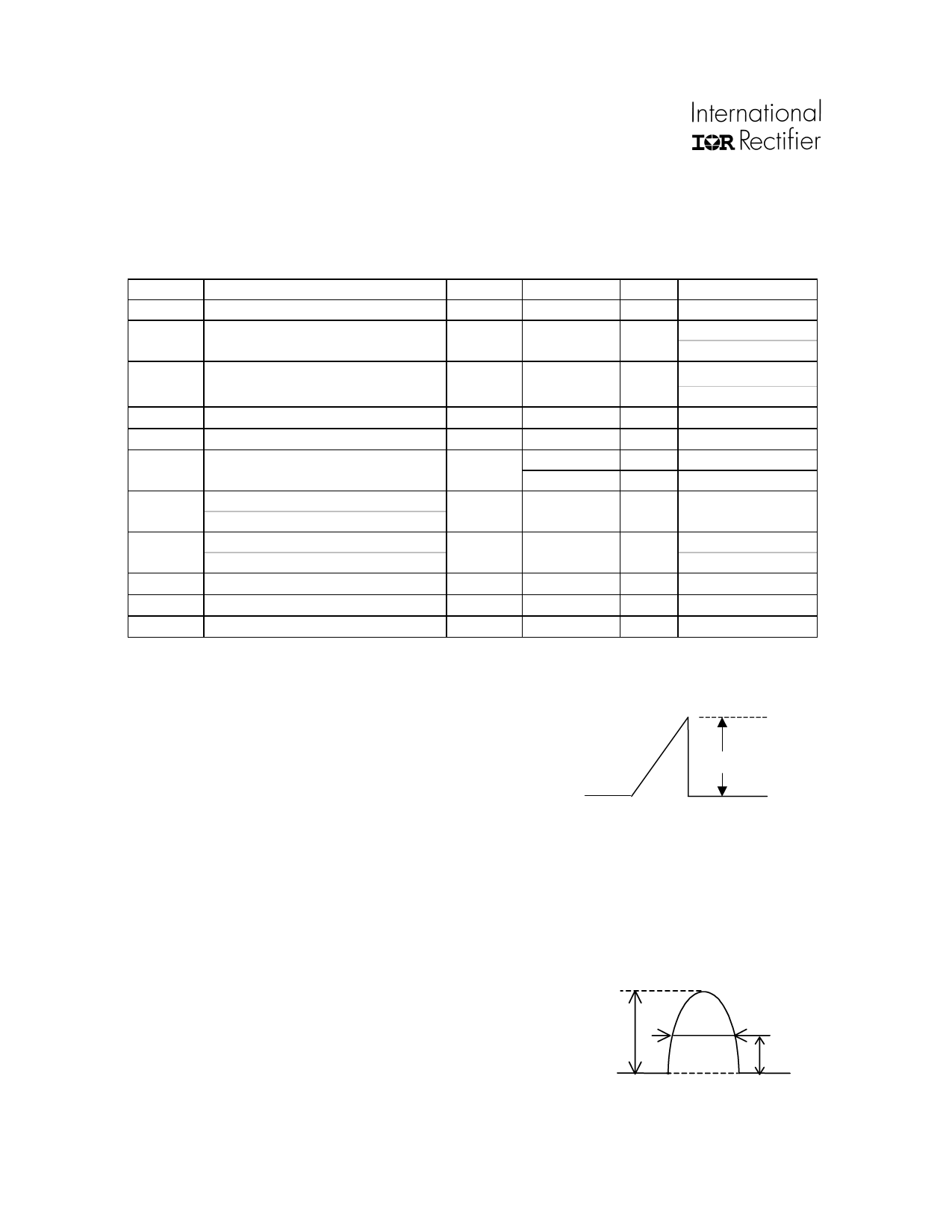
Absolute Maximum Ratings (Ta=25ºC)
Absolute maximum ratings indicate sustained limits beyond which damage to the device may occur. All voltage parameters are
absolute voltages referenced to terminals stated, all currents are defined positive into any lead. The thermal resistance and power
dissipation ratings are measured under board mounted and still air conditions.
Symbol
Definition
IDpeak Drain Current
*1
IDMAX Maximum switching current *5
Terminals Max. Ratings Units
3-2
14
A
3-2
9.7
A
Note
Single Pulse
V2-5=0.78V
Ta=-20~+125℃
Single Pulse
EAS Single pulse avalanche energy *2
3-2
399
mJ
IL peak=4.7A
Vin Input voltage for control part
4-5
35
V
Vth O.C.P/F.B Pin voltage
1-5
6
V
55
W With infintite heatsink
PD1 Power dissipation for MOSFET *3 3-2
2.8
W Without heatsink
Power dissipation for control part
Specified by
PD2
(Control IC) *4
4-5
0.49
W
Vin×Iin
Internal frame temperature
Refer to recommended
TF in operation
-
-20 ~ +125 ℃ operating temperature
Top Operating ambient temperature
-
-20 ~ +125 ℃
Tstg Storage temperature
-
-40 ~ +125 ℃
Tch Channel temperature
-
150
℃
*1 Refer to MOS FET A.S.O curve
*2 MOS FET Tch-EAS curve
*3 Refer to MOS FET Ta-PD1 curve
Fig.1
V2-5
*4 Refer to TF-PD2 curve for Control IC (See page 5)
*5 Maximum switching current.
The maximum switching current is the Drain current determined by the drive voltage of the IC and
threshold voltage (Vth) of MOS FET. Therefore, in the event that voltage drop occurs between Pin 2 and
Pin 5 due to patterning, the maximum switching current decreases as shown by V2-5 in Fig.1
Accordingly please use this device within the decrease value, referring to the derating curve of the
maximum switching current.
1- Recommended operating conditions
Time for input of quasi resonant signals
For the quasi resonant signal inputted to O.C.P/F.B Pin at the time
of quasi resonant operation, the signal shall be wider than Tth(2).
VO.C.P/F.B
0V
Tth(2)≧1.0μsec
Vth(2)
www.irf.com
Share Link: 