5962D0153201TYX Просмотр технического описания (PDF) - Aeroflex UTMC
Номер в каталоге
Компоненты Описание
производитель
5962D0153201TYX Datasheet PDF : 14 Pages
| |||
NC
1
NC
2
A0
3
A1
4
A2
5
A3
6
A4
7
E1
8
DQ0
9
DQ1
10
VDD
11
VSS
12
DQ2
13
DQ3
14
W1
15
A5
16
A6
17
A7
18
A8
19
A9
20
W2
21
NC
22
44
NC
43
E2
42
NC
41
A18
40
A17
39
A16
38
A15
37
G
36
DQ7
35
DQ6
34
VSS
33
VDD
32
DQ5
31
DQ4
30
A14
29
A13
28
A12
27
A11
26
A10
25
NC
24
NC
23
NC
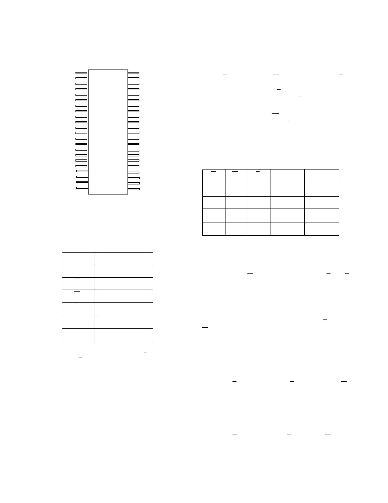
Figure 2. 25ns SRAM Pinout (44)
PIN NAMES
A(18:0)
DQ(7:0)
En
Wn
G
VD D
VSS
Address
Data Input/Output
Device Enable
WriteEnable
Output Enable
Power
Ground
Notes:
1. To avoid bus contention, on the DQ(7:0) bus, only one En can be driven low
simultaneously while G is low.
DEVICE OPERATION
Each die in the UT8Q1024K8 has three control inputs called
Enable (En), Write Enable (Wn), and Output Enable (G); 19
address inputs, A(18:0); and eight bidirectional data lines,
DQ(7:0). The device enable (En) controls device selection,
active, and standby modes. Asserting En enables the device,
causes IDD to rise to its active value, and decodes the 19 address
inputs to each memory die . Wn controls read and write
operations. During a read cycle, G must be asserted to enable
the outputs.
Table 1. Device Operation Truth Table
G
Wn En I/O Mode Mode
X1
X
1 3-state
Standby
X
0
0 Data in Write
1
1
0 3-state
Read2
0
1
0 Data out Read
Notes:
1. “X” is defined as a “don’t care” condition.
2. Device active; outputs disabled.
READ CYCLE
A combination of Wn greater than VIH (min) withEn and G less
than VIL (max) defines a read cycle. Read access time is
measured from the latter of device enable, output enable, or valid
address to valid data output.
SRAM Read Cycle 1, the Address Access is initiated by a change
in address inputs while the chip is enabled with G asserted and
Wn deasserted. Valid data appears on data outputs DQ(7:0) after
the specified tAVQV is satisfied. Outputs remain active
throughout the entire cycle. As long as device enable and output
enable are active, the address inputs may change at a rate equal
to the minimum read cycle time (tAVAV).
SRAM Read Cycle 2, the Chip Enable-controlled Access is
initiated by En going active while G remains asserted, Wn
remains deasserted, and the addresses remain stable for the
entire cycle. After the specified tETQV is satisfied, the eight-bit
word addressed by A(18:0) is accessed and appears at the data
outputs DQ(7:0).
SRAM Read Cycle 3, the Output Enable-controlled Access is
initiated by G going active while En is asserted, Wn is
deasserted, and the addresses are stable. Read access time is
tGLQV unless tAVQV or tETQV have not been satisfied.
2
Share Link: 