NTE787 Просмотр технического описания (PDF) - NTE Electronics
Номер в каталоге
Компоненты Описание
производитель
NTE787 Datasheet PDF : 3 Pages
| |||
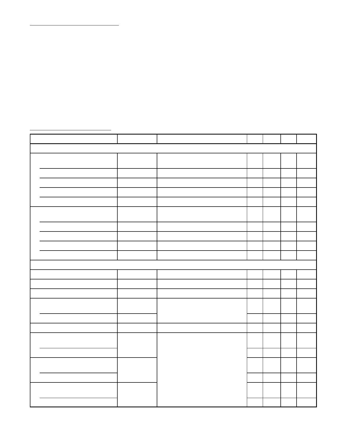
Absolute Maximum Ratings: (TA = +25°C unless otherwise specified)
DC Supply Voltage (Across Pin5 and Pin3, Pin6, Pin13, Pin16 respectively) . . . . . . . . . . . . . . . 16V
DC Current
At Pin3, Pin6, Pin13, Pin16 respectively . . . . . . . . . . . . . . . . . . . . . . . . . . . . . . . . . . . . . . . 10mA
At Pin10 . . . . . . . . . . . . . . . . . . . . . . . . . . . . . . . . . . . . . . . . . . . . . . . . . . . . . . . . . . . . . . . . . . 30mA
Device Dissipation (Up to TA = +50°C), PD . . . . . . . . . . . . . . . . . . . . . . . . . . . . . . . . . . . . . . . . . 760mW
Derate Above TA = +50°C . . . . . . . . . . . . . . . . . . . . . . . . . . . . . . . . . . . . . . . . . . . . . . . 7.6mW/°C
Operating Ambient Temperature Range, Topr . . . . . . . . . . . . . . . . . . . . . . . . . . . . . . . . . . –40° to +85°C
Storage Temperature Range, Tstg . . . . . . . . . . . . . . . . . . . . . . . . . . . . . . . . . . . . . . . . . . –65° to +150°C
Lead Temperature (During Soldering, 1/32” from case, 10sec max), TL . . . . . . . . . . . . . . . . . +265°C
Electrical Characteristics: (TA = +25°C, V+ = 12V unless otherwise specified)
Parameter
Symbol
Test Conditions
Min Typ Max Unit
Static Characteristics
DC Voltage
Pin1, Pin4, Pin9, Pin11
V1, V4, V9, V11
– 0.7 –
V
Pin2, Pin7, Pin8
Pin10
Pin12
Pin15
V2, V7, V8
V10
V12
V15
– 1.4 –
V
– 5.6 –
V
–
0
–
V
– 3.5 –
V
DC Current
Pin3
I3
Pin6
I6
Pin10
I10
– 0.35 – mA
– 1.0 – mA
– 20 – mA
Pin13
I13
Pin16
I16
Dynamic Characteristics
– 0 – mA
– 1.2 – mA
Detector Output
30% Modulation
– 75 – mVrms
Audio Amplifier Gain
AAF
f = 1kHz
– 30 – dB
Audio Distortion
Sensitivity
At Converter Stage Input
At RF Stage Input
VOUT = 100mV
– 0.2 – %
fIN = 1MHz,
– 200 – µV/m
Signal–to–Noise Ratio (S/N) = 20dB – 100 – µV/m
Total Harmonic Distortion
THD
30% Modulation
– 1.0 – %
Input Resistance
At Transistor Q1
At Transistor Q5
RIN
No AGC,
– 3500 –
Ω
Input Frequency Signal (fIN) = 1MHz – 2000 –
Ω
Input Capacitance
At Transistor Q1
CIN
– 17 – pF
At Transistor Q5
– 12 – pF
Feedback Capacitance
At Transistor Q1
CFB
– 1.5 – pF
At Transistor Q5
– 1.5 – pF
Share Link: 