MAX5480A Просмотр технического описания (PDF) - Maxim Integrated
Номер в каталоге
Компоненты Описание
производитель
MAX5480A Datasheet PDF : 7 Pages
| |||
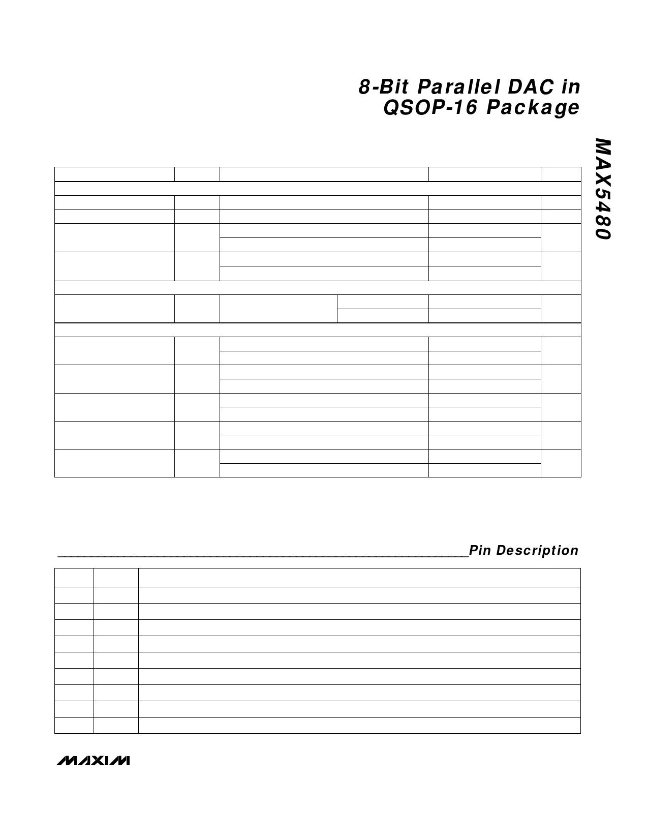
8-Bit Parallel DAC in
QSOP-16 Package
ELECTRICAL CHARACTERISTICS (continued)
(VDD = +5V, VREF = +10V, VOUT1 = VOUT2 = 0V, Circuit of Figure 1, TA = TMIN to TMAX, unless otherwise noted.)
PARAMETER
SYMBOL
CONDITIONS
DIGITAL INPUTS
Input High Voltage
VIH
Input Low Voltage
VIL
Input Current
IIN
TA = +25°C; VIN = 0V to VDD
TA = TMIN to TMAX
Input Capacitance (Note 3)
D0–D7
CIN
WR, CS
POWER REQUIREMENTS
Supply Current
IDD
Digital inputs at 0V or VDD TA = +25°C
TA = TMIN to TMAX
SWITCHING CHARACTERISTICS (Figure 4)
Chip-Select to Write-
Setup Time
MAX5480A
tCS
MAX5480B
Chip-Select to Write-
Hold Time
MAX5480A
tCH
MAX5480B
Write Pulse Width
MAX5480A
tWR
MAX5480B
Data-Setup Time
MAX5480A
tDS
MAX5480B
Data-Hold Time
MAX5480A
tDH
MAX5480B
MIN TYP
2.4
220
35
0
0
220
35
170
55
10
-7
Note 1: Gain error is measured using internal feedback resistor. Full-scale range (FSR) = VREF.
Note 2: Gain TempCo measured from +25°C to TMAX and from +25°C to TMIN.
Note 3: Guaranteed by design.
MAX UNITS
V
0.8
V
±1
µA
±10
8
pF
20
100
µA
500
ns
ns
ns
ns
ns
______________________________________________________________Pin Description
PIN
1
2
3
4–11
12
13
14
15
16
NAME
OUT1
OUT2
GND
D7–D0
CS
WR
VDD
REF
RFB
R-2R Ladder Output
R-2R Ladder Output, complement of OUT1
Ground
Data Inputs, D7 is the most significant bit.
Chip Select Input. Active Low.
Write Control Input. Active Low.
Power Supply Input, +5V
Reference Voltage Input
Feedback Resistor Connection
FUNCTION
_______________________________________________________________________________________ 3
Share Link: 