AD588 Просмотр технического описания (PDF) - Analog Devices
Номер в каталоге
Компоненты Описание
производитель
AD588 Datasheet PDF : 12 Pages
| |||
AD588
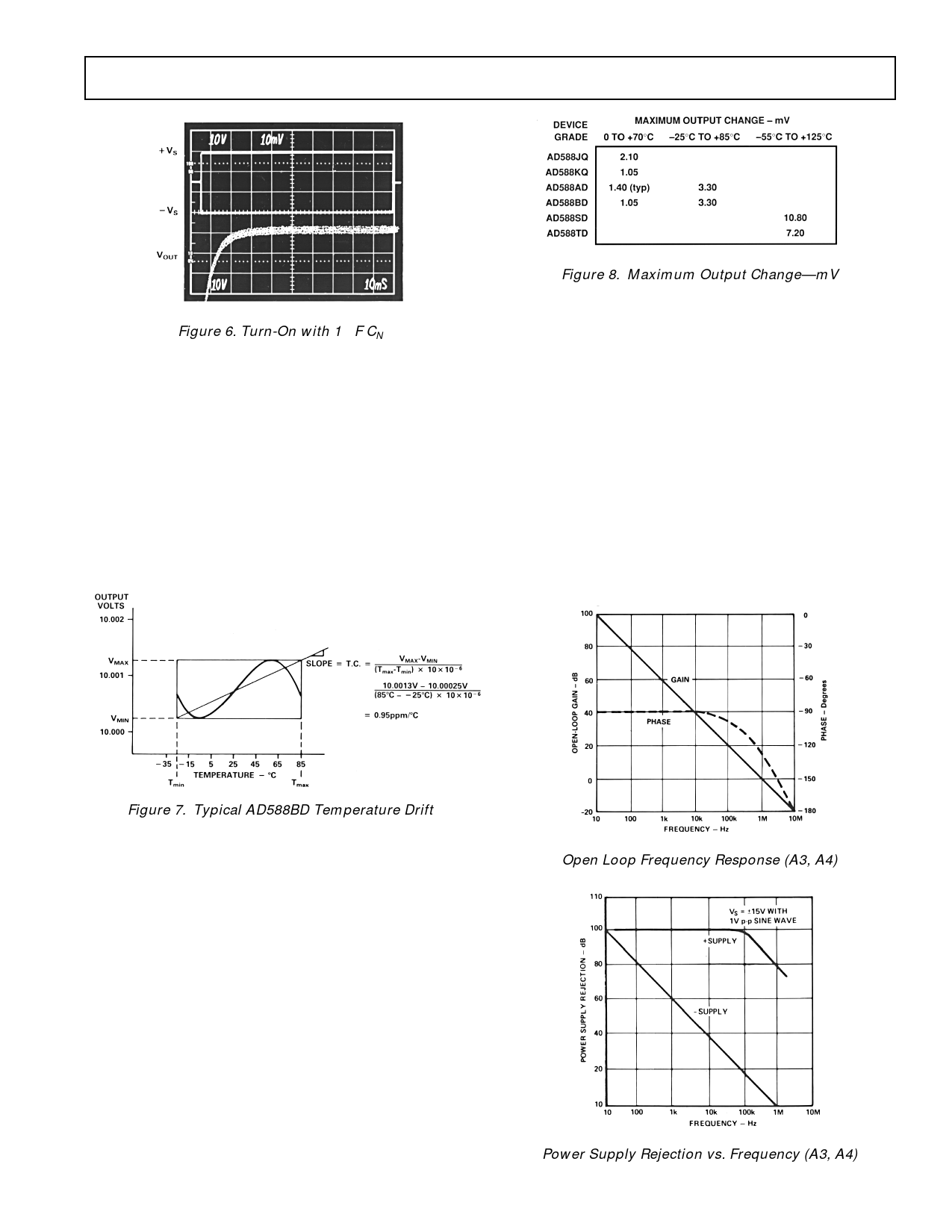
Figure 8. Maximum Output Change—mV
Figure 6. Turn-On with 1 µF CN
TEMPERATURE PERFORMANCE
The AD588 is designed for precision reference applications
where temperature performance is critical. Extensive tempera-
ture testing ensures that the device’s high level of performance is
maintained over the operating temperature range.
Figure 7 shows typical output voltage drift for the AD588BD
and illustrates the test methodology. The box in Figure 7 is
bounded on the sides by the operating temperature extremes
and on top and bottom by the maximum and minimum output
voltages measured over the operating temperature range. The
slope of the diagonal drawn from the lower left corner of the box
determines the performance grade of the device.
KELVIN CONNECTIONS
Force and sense connections, also referred to as Kelvin connec-
tions, offer a convenient method of eliminating the effects of
voltage drops in circuit wires. As seen in Figure 9a, the load cur-
rent and wire resistance produce an error (VERROR = R × IL) at
the load. The Kelvin connection of Figure 9b overcomes the
problem by including the wire resistance within the forcing loop
of the amplifier and sensing the load voltage. The amplifier cor-
rects for any errors in the load voltage. In the circuit shown, the
output of the amplifier would actually be at 10 volts + VERROR
and the voltage at the load would be the desired 10 volts.
The AD588 has three amplifiers which can be used to imple-
ment Kelvin connections. Amplifier A2 is dedicated to the
ground force-sense function while uncommitted amplifiers A3
and A4 are free for other force-sense chores.
In some single-output applications, one amplifier may be unused.
Figure 7. Typical AD588BD Temperature Drift
Each AD588A and B grade unit is tested at –25°C, 0°C, +25°C,
+50°C, +70°C and +85°C. Each AD588S and T grade unit is
tested at –55°C, –25°C, 0°C, +25°C, +50°C, +70°C and
+125°C. This approach ensures that the variations of output
voltage that occur as the temperature changes within the speci-
fied range will be contained within a box whose diagonal has a
slope equal to the maximum specified drift. The position of the
box on the vertical scale will change from device to device as
initial error and the shape of the curve vary. Maximum height of
the box for the appropriate temperature range is shown in Fig-
ure 8. Duplication of these results requires a combination of
high accuracy and stable temperature control in a test system.
Evaluation of the AD588 will produce a curve similar to that in
Figure 7, but output readings may vary depending on the test
methods and equipment utilized.
Open Loop Frequency Response (A3, A4)
REV. B
Power Supply Rejection vs. Frequency (A3, A4)
–6–
Share Link: 