AD588(RevD) Просмотр технического описания (PDF) - Analog Devices
Номер в каталоге
Компоненты Описание
производитель
AD588 Datasheet PDF : 16 Pages
| |||
additional load to the internal Zener diode’s current source,
resulting in a somewhat longer turn-on time. In the case of a
1 µF capacitor, the initial turn-on time is approximately 60 ms
(see Figure 6).
Note: If the NOISE REDUCTION feature is used in the ± 5 V
configuration, a 39 kΩ resistor between Pin 6 and Pin 2 is required
for proper startup.
AD588
DEVICE
MAXIMUM OUTPUT CHANGE – mV
GRADE 0؇C TO +70؇C –25؇C TO +85؇C –55؇C TO +125؇C
AD588JQ
2.10
AD588JQ
1.05
AD588JQ 1.40(typ)
3.30
AD588JQ
1.05
3.30
AD588JQ
10.80
AD588JQ
7.20
Figure 8. Maximum Output Change—mV
Figure 6. Turn-On with CN = 1 F
TEMPERATURE PERFORMANCE
The AD588 is designed for precision reference applications
where temperature performance is critical. Extensive tempera-
ture testing ensures that the device’s high level of performance is
maintained over the operating temperature range.
Figure 7 shows typical output voltage drift for the AD588BD
and illustrates the test methodology. The box in Figure 7 is
bounded on the sides by the operating temperature extremes
and on top and bottom by the maximum and minimum output
voltages measured over the operating temperature range. The
slope of the diagonal drawn from the lower left corner of the
box determines the performance grade of the device.
OUTPUT
VOLTS
10.002
VMAX
10.001
VMIN
10.000
SLOPE = T.C. =
VMAX – VMIN
(TMAX – TMIN ) × 10 × 1–6
10.0013V − 10.00025V
(85°C − –25°C) × 10 × 10–6
–35 –15 5 25 45 65 85
TEMPERATURE – ؇C
Tmin
Tmax
= 0.95ppm / °C
Figure 7. Typical AD588BD Temperature Drift
Each AD588A and B grade unit is tested at –25°C, 0°C, +25°C,
+50°C, +70°C, and +85°C. This approach ensures that the
variations of output voltage that occur as the temperature changes
within the specified range will be contained within a box whose
diagonal has a slope equal to the maximum specified drift. The
position of the box on the vertical scale will change from device
to device as initial error and the shape of the curve vary. Maxi-
mum height of the box for the appropriate temperature range is
shown in Figure 8. Duplication of these results requires a combi-
nation of high accuracy and stable temperature control in a test
system. Evaluation of the AD588 will produce a curve similar to
that in Figure 7, but output readings may vary depending on the
test methods and equipment utilized.
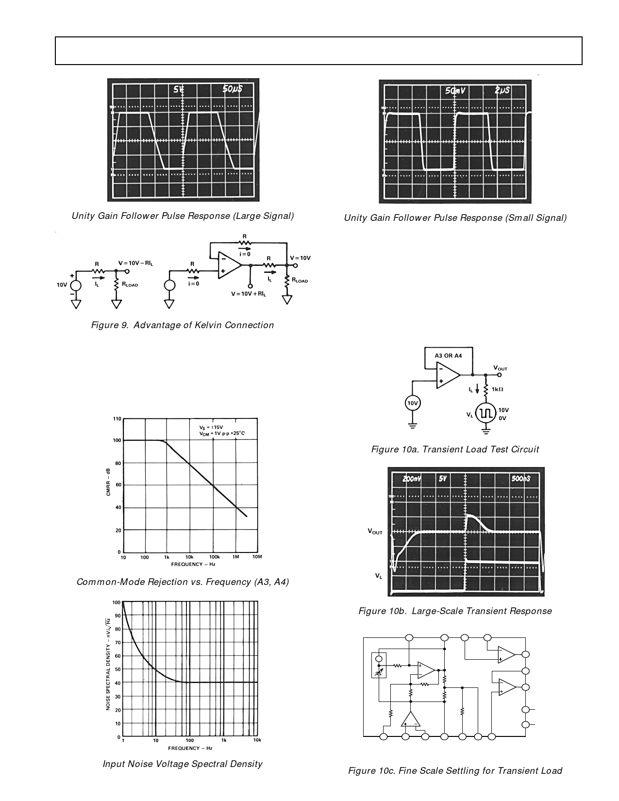
KELVIN CONNECTIONS
Force and sense connections, also referred to as Kelvin connec-
tions, offer a convenient method of eliminating the effects of
voltage drops in circuit wires. As seen in Figure 9, the load
current and wire resistance produce an error (VERROR = R × IL) at
the load. The Kelvin connection of Figure 9 overcomes the
problem by including the wire resistance within the forcing loop
of the amplifier and sensing the load voltage. The amplifier
corrects for any errors in the load voltage. In the circuit shown,
the output of the amplifier would actually be at 10 V + VERROR and
the voltage at the load would be the desired 10 V.
The AD588 has three amplifiers that can be used to implement
Kelvin connections. Amplifier A2 is dedicated to the ground
force-sense function, while uncommitted amplifiers A3 and A4
are free for other force-sense chores.
R
+
10V
–
R V = 10V – RIL
IL
RLOAD
R
I=0
I=0
V = 10V
IL
RLOAD
V = 10V + RIL
Figure 9. Advantage of Kelvin Connection
In some single-output applications, one amplifier may be unused.
In such cases, the unused amplifier should be connected as a
unity-gain follower (force + sense pin tied together), and the
input should be connected to ground.
An unused amplifier section may be used for other circuit functions
as well. Figures 10 through 14 show the typical performance of
A3 and A4.
100
0
80
–30
GAIN
60
–60
40
PHASE
20
–90
–120
0
–150
–20
–180
10
100
1k
10k
100k
1M
10M
FREQUENCY – Hz
Figure 10. Open-Loop Frequency Response (A3, A4)
REV. D
–7–
Share Link: 