AD588(RevD) Просмотр технического описания (PDF) - Analog Devices
Номер в каталоге
Компоненты Описание
производитель
AD588 Datasheet PDF : 16 Pages
| |||
AD588
0.1F
0.1F
NOISE
REDUCTION
Note that a second capacitor is needed in order to implement
the NOISE REDUCTION feature when using the AD588 in
the –10 V mode (Figure 2c.). The NOISE REDUCTION capaci-
tor is limited to 0.1 µF maximum in this mode.
RB
A1
R1
R2
R3
A2
R4
R5
R6
A3
A4
+VS
AD588
–VS
SYSTEM
GROUND
–5V
–10V
+15V
0.1F
SYSTEM
GROUND
0.1F
–15V
Figure 2c. –10 V Output
Trimming the AD588 introduces no additional errors over
temperature, so precision potentiometers are not required.
For single-output voltage ranges, or in cases when BALANCE
ADJUST is not required, Pin 12 should be connected to Pin 11.
If GAIN ADJUST is not required, Pin 5 should be left floating.
NOISE PERFORMANCE AND REDUCTION
The noise generated by the AD588 is typically less than 6 µV p-p
over the 0.1 Hz to 10 Hz band. Noise in a 1 MHz bandwidth is
approximately 600 µV p-p. The dominant source of this noise is
the buried Zener, which contributes approximately 100 nV/√Hz.
In comparison, the op amp’s contribution is negligible. Figure 3
shows the 0.1 Hz to 10 Hz noise of a typical AD588.
Figure 4. Effect of 1 µF Noise Reduction Capacitor
on Broadband Noise
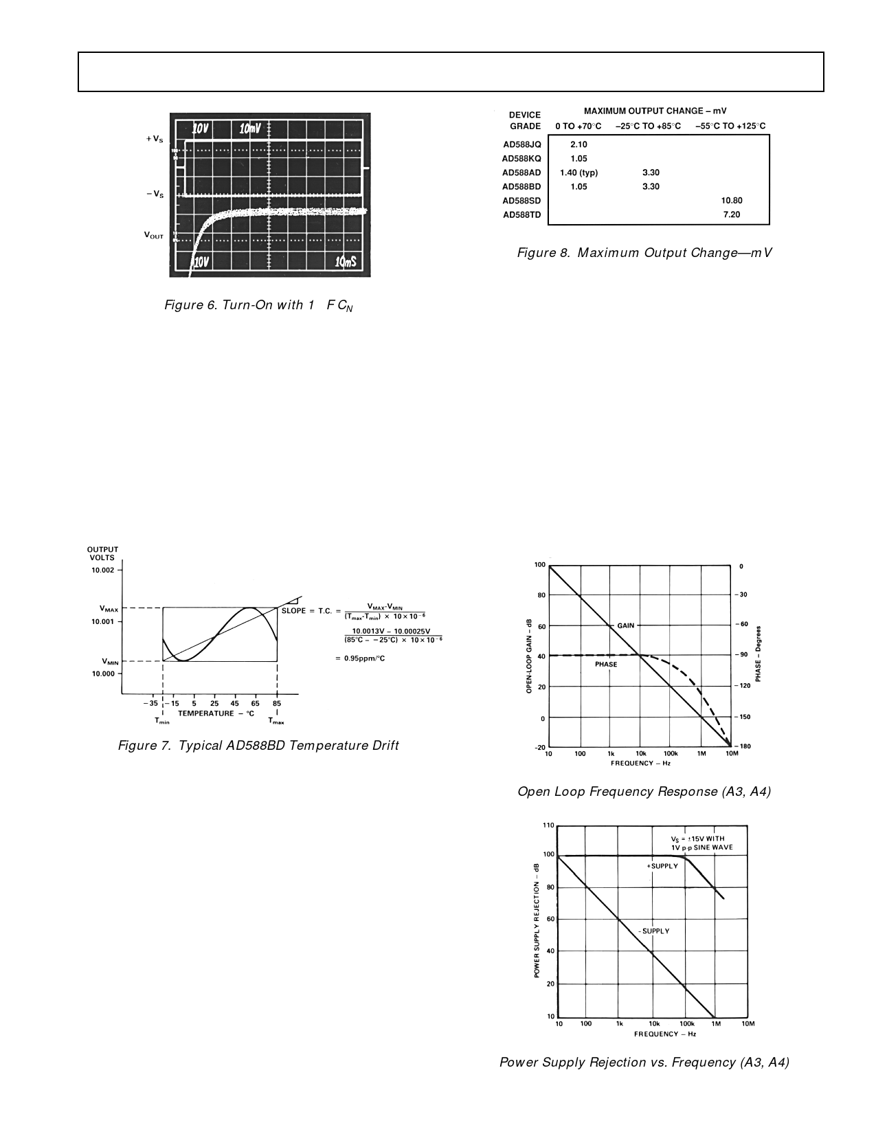
TURN-ON TIME
Upon application of power (cold start), the time required for the
output voltage to reach its final value within a specified error
band is the turn-on settling time. Two components normally
associated with this are: time for active circuits to settle and
time for thermal gradients on the chip to stabilize. Figures 5a
and 5b show the turn-on characteristics of the AD588. It
shows the settling to be about 600 µs. Note the absence of any
thermal tails when the horizontal scale is expanded to 2 ms/cm in
Figure 5b.
Figure 5a. Electrical Turn-On
Figure 3. 0.1 Hz to 10 Hz Noise (0.1 Hz to 10 Hz BPF
with Gain of 1000 Applied)
If further noise reduction is desired, an optional capacitor, CN,
may be added between the NOISE REDUCTION pin and ground,
as shown in Figure 2b. This will form a low-pass filter with the
4 kΩ RB on the output of the Zener cell. A 1 µF capacitor will
have a 3 dB point at 40 Hz and will reduce the high frequency
(to 1 MHz) noise to about 200 µV p-p. Figure 4 shows the 1 MHz
noise of a typical AD588 both with and without a 1 µF capacitor.
Figure 5b. Extended Time Scale Turn-On
Output turn-on time is modified when an external noise reduc-
tion capacitor is used. When present, this capacitor presents an
–6–
REV. D
Share Link: 