FT120 Просмотр технического описания (PDF) - Future Technology
Номер в каталоге
Компоненты Описание
производитель
FT120 Datasheet PDF : 40 Pages
| |||
Document No.: FT_000646
FT120 USB DEVICE CONTROLLER WITH PARALLEL BUS IC
Datasheet Version 1.2
USB Protocol Engine. The USB Protocol Engine manages the data streamClefraormantchee Ndoev.:icFeTUDSIB# c2o9n1trol
endpoint. It handles the low level USB protocol requests generated by the USB host controller. The
Protocol Engine also includes a memory management unit which handles endpoint buffers.
OUT Buffer. Data sent from the USB host controller to FT120 via the USB data OUT endpoint is stored in
the OUT buffer. Data is removed from the OUT buffer to system memory under control of the parallel
interface block.
IN Buffer. Data from system memory is stored in the IN buffer. The USB host controller removes data
from the IN buffer by sending a USB request for data from the device data IN endpoint.
RESET Generator. The integrated Reset Generator cell provides a reliable power-on reset to the device
internal circuitry at power up. The RESET_n input pin allows an external device to reset the FT120.
Parallel Interface Block. The 8-bit parallel bus allows direct interface to a generic microcontroller
(MCU), supporting both multiplexed and non-multiplexed address/data bus configurations. The FT120
also supports Direct Memory Access (DMA) operation. With DMA access data can be written to the IN
buffer or read from the OUT buffer without MCU intervention. The DMA access can be done in single cycle
or burst mode.
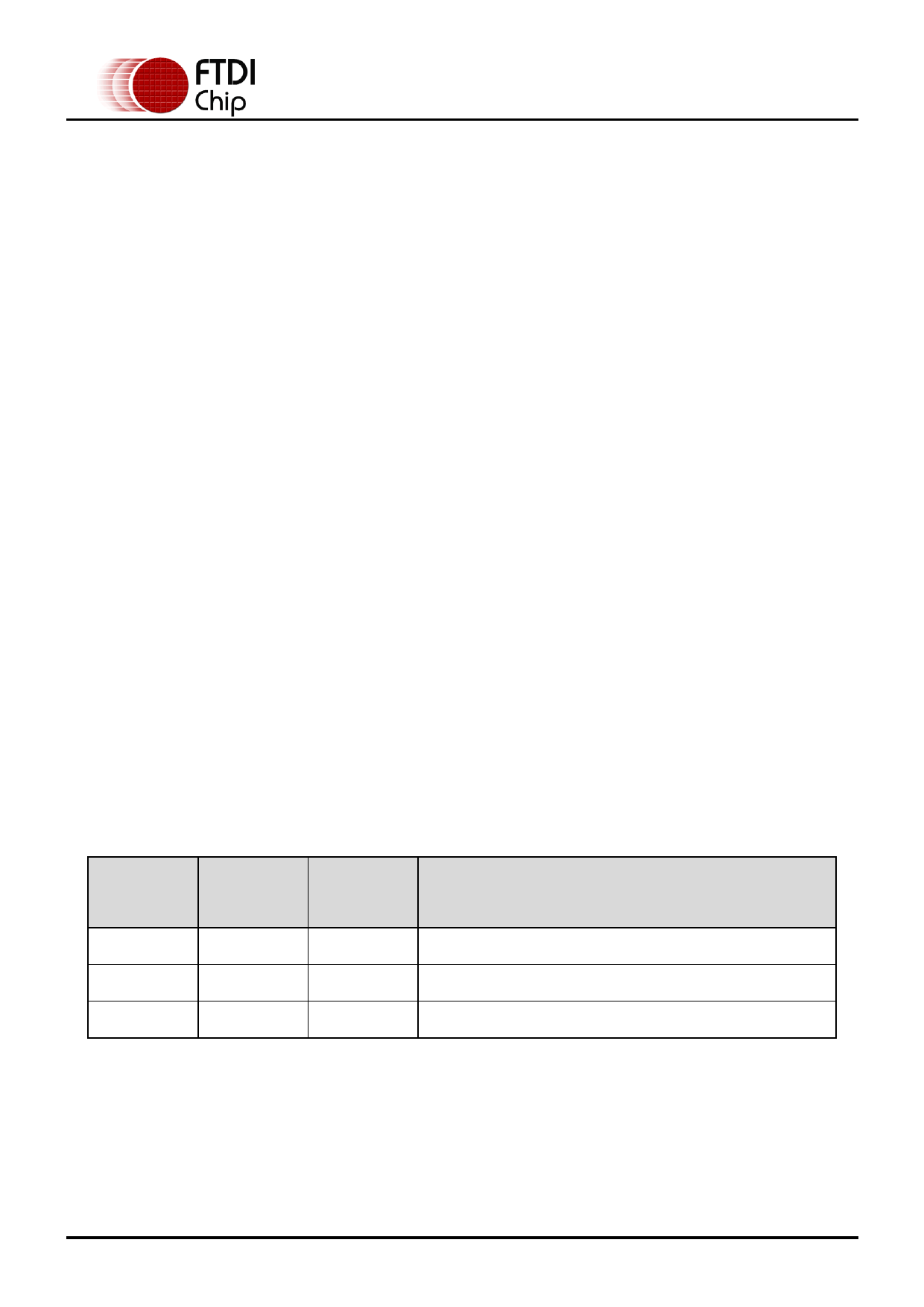
4.2 Interrupt Modes
The FT120 interrupt pin (INT_n) can be programmed to generate an interrupt in different modes. The
interrupt source can be any bit in the Interrupt Register, an SOF packet being received, or both. The
interrupt modes are selectable by two register bits, one is the SOF-only Interrupt Mode bit (bit 7 of Clock
Division Factor register), and the other is the Interrupt Pin Mode bit (bit 5 of DMA Configuration register).
Interrupt
mode
Bit SOF-only
Interrupt
Mode
Bit Interrupt
Pin Mode
0
0
0
1
0
1
2
1
X
Table 4-1 Interrupt modes
Interrupt source
Any bit in Interrupt register
Any bit in Interrupt register and SOF
SOF only
Copyright © 2014 Future Technology Devices International Limited
10
Share Link: 