MAX8564 –Я—А–Њ—Б–Љ–Њ—В—А —В–µ—Е–љ–Є—З–µ—Б–Ї–Њ–≥–Њ –Њ–њ–Є—Б–∞–љ–Є—П (PDF) - Maxim Integrated
–Э–Њ–Љ–µ—А –≤ –Ї–∞—В–∞–ї–Њ–≥–µ
–Ъ–Њ–Љ–њ–Њ–љ–µ–љ—В—Л –Ю–њ–Є—Б–∞–љ–Є–µ
–њ—А–Њ–Є–Ј–≤–Њ–і–Є—В–µ–ї—М
MAX8564 Datasheet PDF : 15 Pages
| |||
±1%, Ultra-Low Output Voltage, Dual and Triple
Linear n-FET Controllers
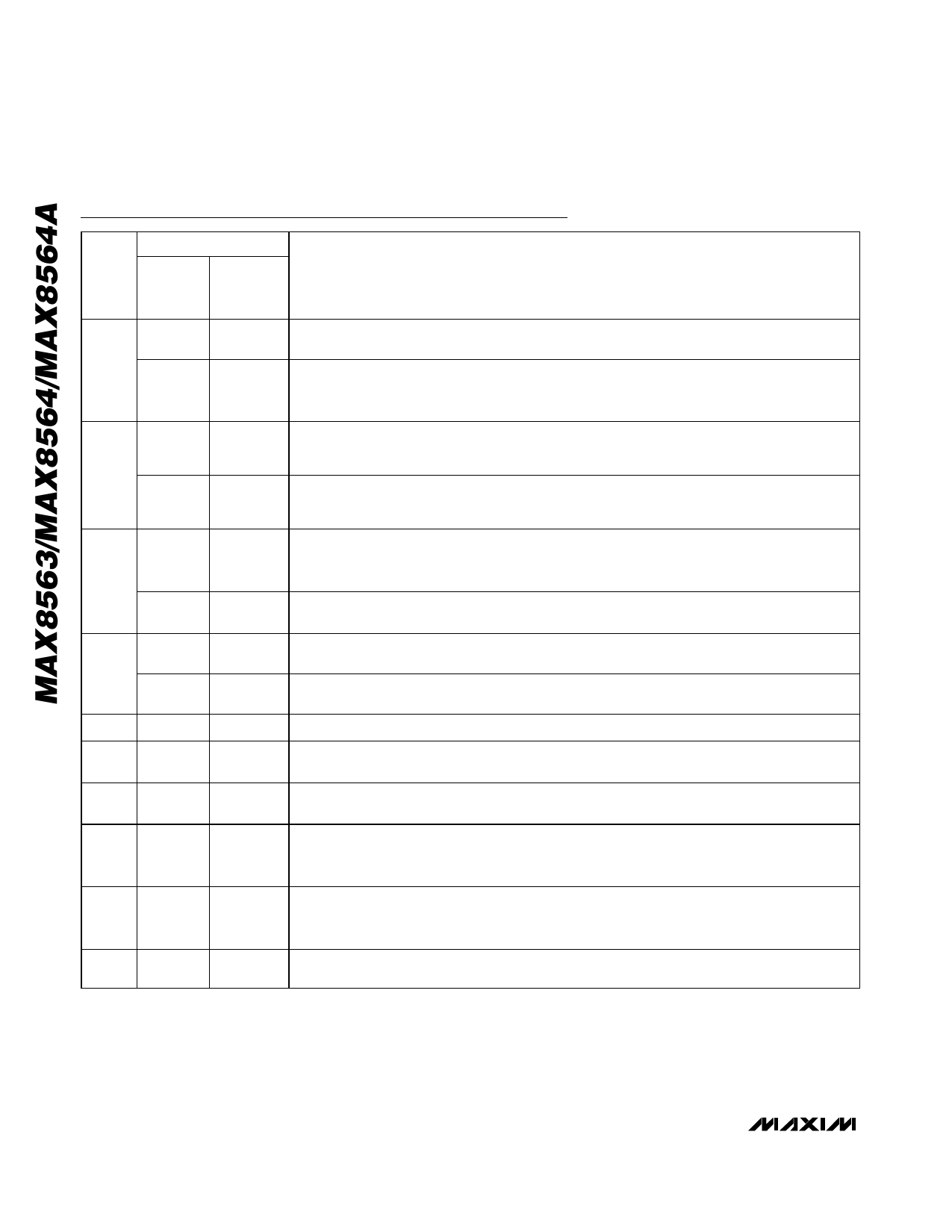
Pin Description (continued)
NAME
PIN
MAX8563
MAX8564/
MAX8564A
FUNCTION
вАФ
7
DRV3
вАФ
8
FB3
вАФ
9
EN3
вАФ
10
POK3
11
N.C.
12
POK2
13
EN2
14
FB2
15
DRV2
16
VDD
EN2
вАФ
FB2
вАФ
DRV2
вАФ
VDD
вАФ
вАФ
вАФ
вАФ
вАФ
вАФ
вАФ
Enable Control for Output 2. Drive logic high to enable output 2, or logic low to disable the
output. Connect to VDD for always-on operation.
Output 3 n-MOSFET Drive. Drives the gate of an external n-channel MOSFET to regulate output 3.
DRV3 is internally pulled to ground when EN3 is logic low. Connect an external series RC circuit
for compensation. See the Stability Compensation section.
Feedback Input for Output 2. Connect to the center of a resistor-divider between output 2 and
GND to set the output voltage of output 2. The feedback regulation voltage is 0.500V. See the
Output Voltage Setting section.
Feedback Input for Output 3. Connect to the center of a resistor-divider between output 3 and
GND to set the output voltage of output 3. The feedback regulation voltage is 0.500V. See the
Output Voltage Setting section.
Output 2 n-MOSFET Drive. Drives the gate of the external n-channel MOSFET to regulate output 2.
DRV2 is internally pulled to ground when EN2 is logic low. Connect an external series RC circuit
for compensation. See the Stability Compensation section.
Enable Control for Output 3. Drive logic high to enable output 3, or logic low to disable the
output. Connect to VDD for always-on operation.
+5V or +12V Supply Input. Connect to external +5V or +12V supply rail. Bypass with a 0.1µF
ceramic or larger capacitor.
Output 3 Power-Good Signal. Open-drain output pulls low when output 3 is 12% below the
nominal regulated voltage.
No Internal Connection
Output 2 Power-Good Signal. Open-drain output pulls low when output 2 is 12% below the
nominal regulated voltage.
Enable Control for Output 2. Drive logic high to enable output 2, or logic low to disable the
output. Connect to a VDD for always-on operation.
Feedback Input for Output 2. Connect to the center of a resistor-divider between output 2 and
GND to set the output voltage of output 2. The feedback regulation voltage is 0.500V. See the
Output Voltage Setting section.
Output 2 n-MOSFET Drive. Drives the gate of the external n-channel MOSFET to regulate output 2.
DRV2 is internally pulled to ground when EN2 is logic low. Connect an external series RC circuit
for compensation. See the Stability Compensation section.
+5V or +12V Supply Input. Connect to an external +5V or +12V supply rail. Bypass with a 0.1µF
ceramic or larger capacitor.
6 _______________________________________________________________________________________
Share Link: 