MAX3816ACUE Просмотр технического описания (PDF) - Maxim Integrated
Номер в каталоге
Компоненты Описание
производитель
MAX3816ACUE Datasheet PDF : 18 Pages
| |||
I2C 2-Wire Extender for DDC in DVI,
HDMI, and VGA Interfaces
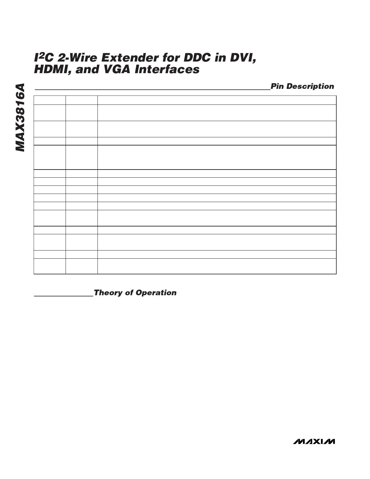
Pin Description
PIN
1
2
3
4
5
6
7
8, 9, 10
11
12
13
14
15
16
NAME
FUNCTION
DRVR_EN
Driver Enable Input, LVTTL/LVCMOS. Set high to enable all data and clock drivers for normal
operation. Set low to disable drivers, permitting isolation of cable bus from display bus.
VCC
CLOCK_C
Power Supply for Cable Side. In the DDC application, connect to DDC +5V. Connect 10μF or larger
bypass capacitor as shown in Figure 6.
I2C Cable-Side Clock with Cable Driver, CMOS Input/Output. Connect a 47k pullup resistor to VCC.
GND_REF
DATA_C
GND_REF
VCC
DNC
VDD
DATA_D
VSS
CLOCK_D
VSS_T
MODE
Cable-Side Ground Return. Connect directly to cable DDC ground wire. The MAX3816A circuitry uses
the video source DDC GND as a threshold reference. Also connect 10μF or larger bypass capacitors
as shown in Figure 6.
I2C Cable-Side Data with Cable Driver, CMOS Input/Output. Connect a 47k pullup resistor to VCC.
Cable-Side Ground Return (Alternate). Connected internally to pin 4 above.
Power Supply for Cable Side (Alternate). Connected internally to pin 2 above.
Do Not Connect
Power Supply for Display Side and Core Circuitry. Connect bypass capacitor as shown in Figure 6.
I2C Display-Side Data, CMOS Input/Output. Connect a 2.2k pullup resistor to VDD for VDD = 3.3V,
or a 3.3k pullup resistor to VDD for VDD = 5V.
Ground for Display Side and Core Circuitry. Connect bypass capacitors as shown in Figure 6.
I2C Display-Side Clock, CMOS Input/Output. Connect a 2.2k pullup resistor to VDD for VDD = 3.3V,
or a 3.3k pullup resistor to VDD for VDD = 5V.
Must Be Connected to VSS for Normal Operation
Mode Setting Input, LVTTL/LVCMOS. Force high for parallel mode (normal operation) and force low for
serial operation.
Theory of Operation
The MAX3816A has parallel and series modes. The
parallel mode is preferred for applications where high
tolerance to noncompliant source and sink devices is
desired (noncompliant VOL from displays and noncom-
pliant VIH from sources are common). Further, the par-
allel mode can be operated with other speed-up
devices on the same bus, either active (DRVR_EN = HI)
or in bypass (DRVR_EN = LO).
Series mode is preferred for applications where high
tolerance to ground offset or noise between and source
and sink is needed. Series mode also isolates display
circuits from transmission line reflections in very long
cables, providing full isolation between cable and dis-
play buses. For in-display applications, series mode
can provide level shifting between the 5V cable DDC
and 3.3V display internal DDC.
A single MAX3816A is applied at the display side of the
video link to compensate for excessive cable capaci-
tance. The overall operation of the MAX3816A, for
either the DATA or CLOCK signal, can be summarized
as follows (Figures 1a and 1b).
1) High state. Drivers off. Level sensing on.
If no client device is controlling the “wired-AND” bus
from either the source or display side, all device dri-
vers are off and the bus (including the MAX3816A)
is waiting in the high state. The pullup resistors on
each side are holding the bus up to VCC on the
source side and VDD on the display side.
2) High-to-low transition. Drivers assert low. Level
sensing off (Holdoff).
A change of state is initiated by any device driver
pulling low. Once the signal transitions below 75%
of the power supply, the MAX3816A drives both the
source and display sides toward ground with a low-
impedance driver, level sensing is turned off, and
the holdoff timer is started. The source side is
pulled down to the level of the VSS. This is accom-
plished using a low-impedance n-channel buffer
that is designed to drive a 1 meter (60pF) to 60
6 _______________________________________________________________________________________
Share Link: 