ISL83080E –ü—Ä–æ—Å–º–æ—Ç—Ä —Ç–µ—Ö–Ω–∏—á–µ—Å–∫–æ–≥–æ –æ–ø–∏—Å–∞–Ω–∏—è (PDF) - Intersil
–ù–æ–º–µ—Ä –≤ –∫–∞—Ç–∞–ª–æ–≥–µ
–ö–æ–º–ø–æ–Ω–µ–Ω—Ç—ã –û–ø–∏—Å–∞–Ω–∏–µ
–ø—Ä–æ–∏–∑–≤–æ–¥–∏—Ç–µ–ª—å
ISL83080E Datasheet PDF : 20 Pages
| |||
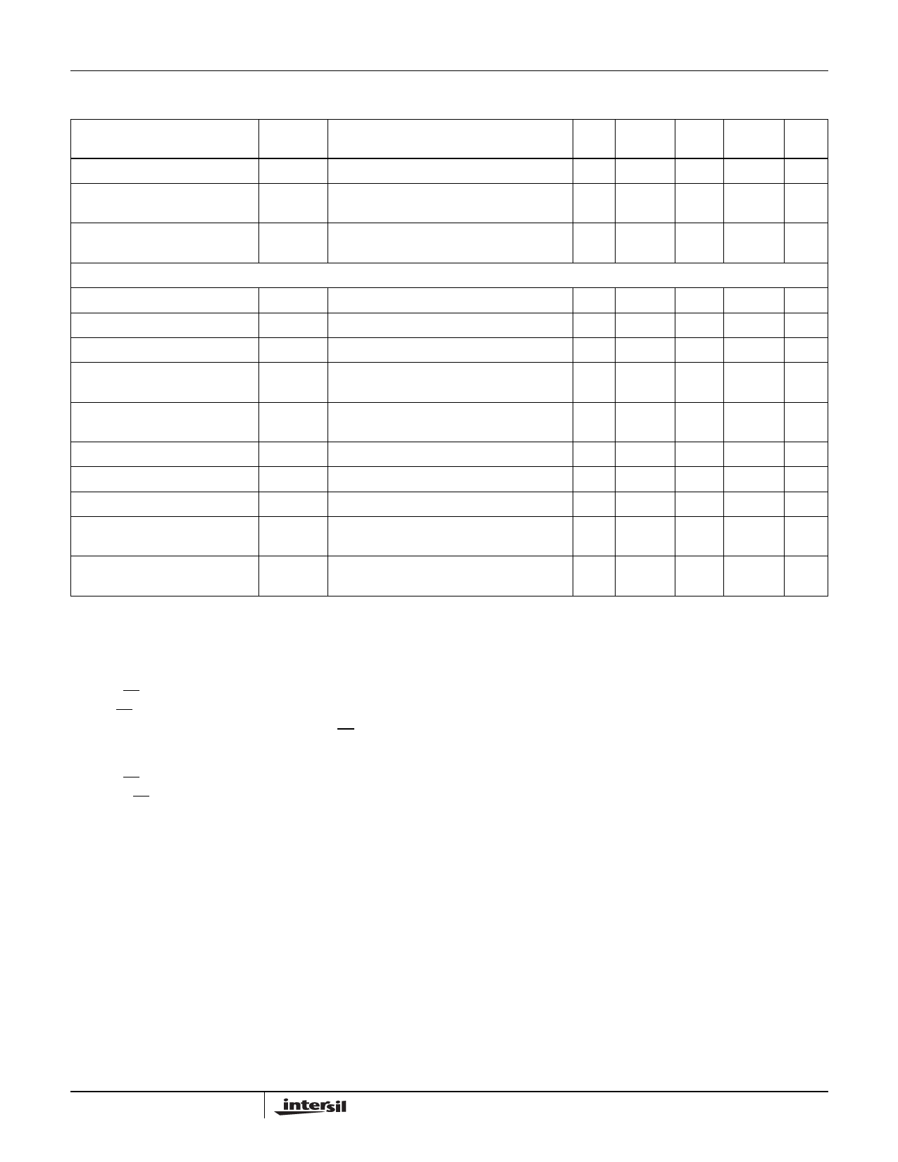
ISL83080E, ISL83082E, ISL83083E, ISL83084E, ISL83085E, ISL83086E, ISL83088E
Electrical Specifications Test Conditions: VCC = 4.5V to 5.5V; Unless Otherwise Specified. Typicals are at VCC = 5V, TA = +25°C
(Note 4). (Continued)
PARAMETER
SYMBOL
TEST CONDITIONS
TEMP MIN
MAX
(°C) (Note 12) TYP (Note 12) UNITS
Time to Shutdown
tSHDN (Notes 9, 13)
Full
60
Receiver Enable from Shutdown to tZH(SHDN) RL = 1kΩ, CL = 15pF, SW = GND (Figure 6), Full
-
Output High
(Notes 9, 11, 13)
160
600
ns
150
2000
ns
Receiver Enable from Shutdown to tZL(SHDN) RL = 1kΩ, CL = 15pF, SW = VCC (Figure 6), Full
-
Output Low
(Notes 9, 11, 13)
150
2000
ns
RECEIVER SWITCHING CHARACTERISTICS (10Mbps Versions; ISL83086E, ISL83088E)
Maximum Data Rate
fMAX (Figure 5)
Full
10
Receiver Input to Output Delay
tPLH, tPHL (Figure 5)
Full
-
Receiver Skew | tPLH - tPHL |
tSKD (Figure 5)
Full
-
Receiver Enable to Output Low
tZL
RL = 1kΩ, CL = 15pF, SW = VCC (Figure 6) Full
-
(Note 8)
15
-
Mbps
70
125
ns
0
10
ns
10
30
ns
Receiver Enable to Output High
tZH
RL = 1kΩ, CL = 15pF, SW = GND (Figure 6) Full
-
(Note 8)
10
30
ns
Receiver Disable from Output Low
tLZ
RL = 1kΩ, CL = 15pF, SW = VCC (Figure 6) Full
-
Receiver Disable from Output High
tHZ
RL = 1kΩ, CL = 15pF, SW = GND (Figure 6) Full
-
Time to Shutdown
tSHDN (Notes 9, 11)
Full
60
Receiver Enable from Shutdown to tZH(SHDN) RL = 1kΩ, CL = 15pF, SW = GND (Figure 6) Full
-
Output High
(Notes 9, 11)
10
30
ns
10
30
ns
160
600
ns
150
2000
ns
Receiver Enable from Shutdown to tZL(SHDN) RL = 1kΩ, CL = 15pF, SW = VCC (Figure 6) Full
-
Output Low
(Notes 9, 11)
150
2000
ns
NOTES:
4. All currents into device pins are positive; all currents out of device pins are negative. All voltages are referenced to device ground unless
otherwise specified.
5. Supply current specification is valid for loaded drivers when DE = 0V.
6. Applies to peak current. See “Typical Performance Curves” beginning on page 13 for more information.
7. Keep RE = 0 to prevent the device from entering SHDN.
8. The RE signal high time must be short enough (typically <100ns) to prevent the device from entering SHDN.
9. Transceivers are put into shutdown by bringing RE high and DE low. If the inputs are in this state for less than 60ns, the parts are guaranteed
not to enter shutdown. If the inputs are in this state for at least 600ns, the parts are guaranteed to have entered shutdown. See “Low Power
Shutdown Mode” on page 12.
10. Keep RE = VCC, and set the DE signal low time >600ns to ensure that the device enters SHDN.
11. Set the RE signal high time >600ns to ensure that the device enters SHDN.
12. Parts are 100% tested at +25°C. Temperature limits established by characterization and are not production tested.
13. Does not apply to the ISL83084E.
8
FN6085.8
February 27, 2008
Share Link: 