NTA0509M Просмотр технического описания (PDF) - C AND D TECHNOLOGIES
Номер в каталоге
Компоненты Описание
производитель
NTA0509M Datasheet PDF : 2 Pages
| |||
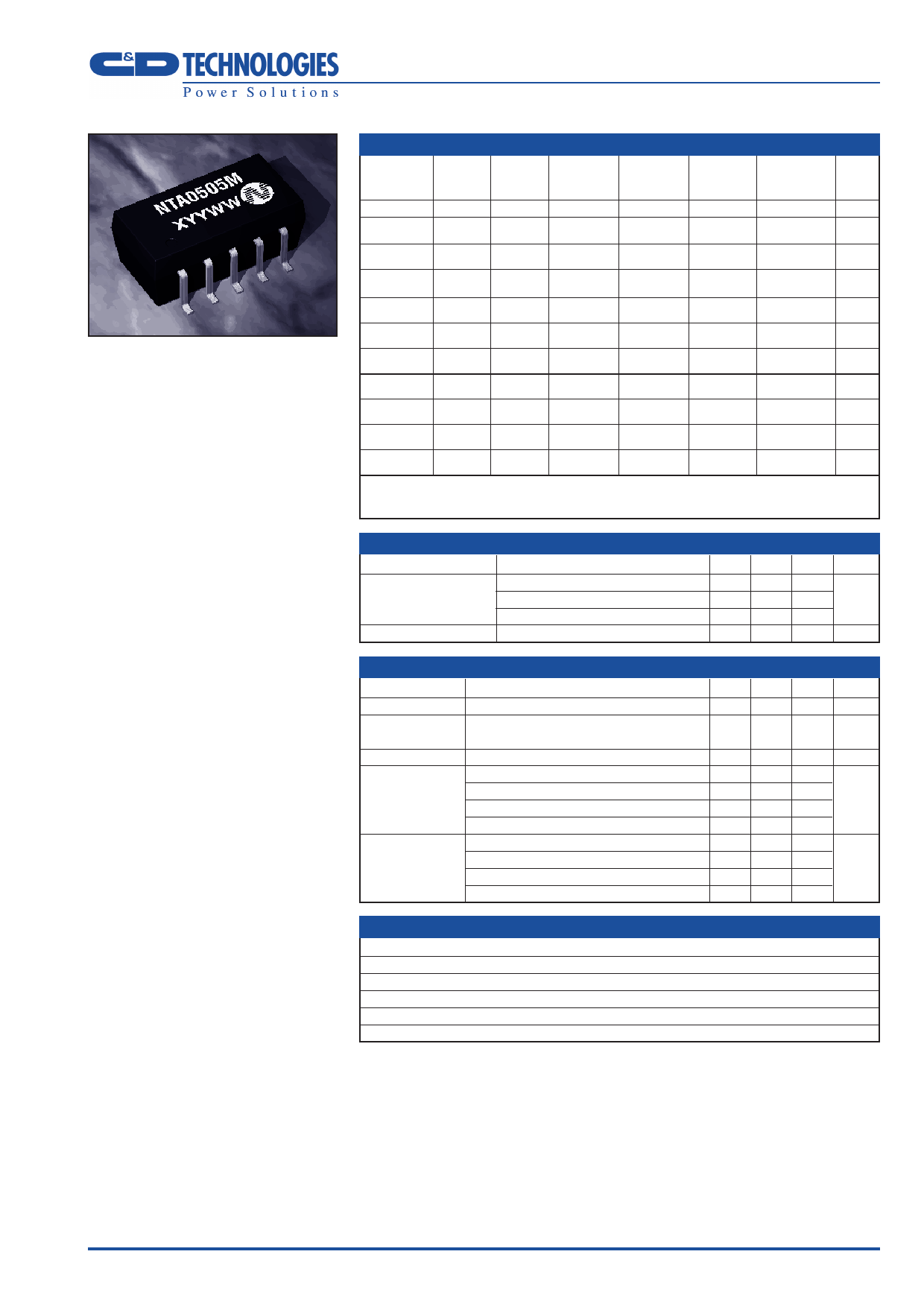
NTA SERIES
Isolated 1W Dual Output SM DC-DC Converters
FEATURES
■ Wide Temperature Performance at
Full 1Watt Load, -40°C to 85°C
■ Lead Frame Technology
■ CECC00802 Reflow (280°C)
■ Dual Isolated Output
■ 1kVDC Isolation
■ Efficiency to 78%
■ Power Density 1.36W/cm3
■ 5V & 12V Input
■ 5V, 9V, 12V and 15V Output
■ Footprint Over Pins 1.64cm2
■ UL 94V-0 Package Material
■ No Heatsink Required
■ Internal SMD Construction
■ Toroidal Magnetics
■ Plastic Encapsulated
■ MTTF up to 2.1 Million Hours
■ Custom Solutions Available
■ Multi Layer Ceramic Capacitors
■ Lead Free Compatible
DESCRIPTION
The NTA series of miniature surface mounted
DC-DC Converters employ leadframe
technology and transfer moulding techniques
to bring all of the benefits of IC style
packaging to hybrid circuitry. The devices are
fully compatible with CECC00802 to 280°C
which allows them to be placed and reflowed
with IC’s, thus reducing time and cost in
production. Co-planarity of the lead positions
is based upon IEC 191-6:1990. The devices
are suitable for all applications where high
volume production is envisaged.
SELECTION GUIDE
Nominal
Input Output
Voltage Voltage
Order Code5 (V)
(V)
NTA0312M 3.3
12
NTA0315M 3.3
15
Output
Current
(mA)
±42
±33
Input
Current at
Rated Load Efficiency
(mA)
(%)
390
77
392
77
Isolation
Capacitance MTTF1
(pF)
kHrs
40
375
42
206
NTA0505M
5
5
±100
290
69
33
1697
NTA0509M
5
9
±55
267
75
38
682
NTA0512M
5
12
±42
260
77
44
343
NTA0515M
5
15
±33
256
78
43
188
NTA1205M 12
5
±100
121
69
50
559
NTA1209M 12
9
±55
113
74
72
375
NTA1212M 12
12
±42
111
75
89
243
NTA1215M 12
15
±33
110
76
100
154
When operated with additional external load capacitance the rise time of the input voltage will determine the
maximum external capacitance value for guaranteed start up. The slower the rise time of the input voltage the
greater the maximum value of the additional external capacitance for reliable start up.
INPUT CHARACTERISTICS
Parameter
Conditions
MIN TYP MAX Units
Continuous operation, 3V input types 2.97 3.3 3.63
Voltage Range
Continuous operation, 5V input types 4.5 5 5.5 V
Continuous operation, 12V input types 10.8 12 13.2
Reflected Ripple Current
41 47 mA p-p
OUTPUT CHARACTERISTICS
Parameter
Rated Power2
Voltage Set Point
Accuracy
Line regulation
Load Regulation3
Ripple and Noise
Conditions
TA = -40°C to 85°C
See tolerance envelope
High VIN to low VIN
10% load to rated load, 5V output types
10% load to rated load, 9V output types
10% load to rated load, 12V output types
10% load to rated load, 15V output types
BW=DC to 20MHz, 5V output types
BW=DC to 20MHz, 9V output types
BW=DC to 20MHz, 12V output types
BW=DC to 20MHz, 15V output types
MIN TYP MAX Units
1.0 W
1.0 1.2 %/%
10 12
6.5 8
%
6.0 8.5
6.0 7.0
50 100
35 80 mV p-p
50 110
65 110
ABSOLUTE MAXIMUM RATINGS
Short circuit duration4
Internal power dissipation
Lead temperature 1.5mm from case for 10 seconds
Input Voltage VIN , NTA03 types
Input Voltage VIN , NTA05 types
Input voltage VIN , NTA12 types
1second
550mW
300°C
5.5V
7V
15V
1 Calculated using MIL-HDBK-217F with nominal input voltage at full load.
2 See derating curve.
3 12V input types have typically 3% less load regulation change.
4 Supply voltage must be discontinued at the end of the short circuit duration.
5 If components are required in tape and reel format suffix order code with -R, e.g. NTA0505M-R
All specifications typical at TA=25°C, nominal input voltage and rated output current unless otherwise specified.
www.cdpoweronline.com
Share Link: 