FKC08W(2008) Просмотр технического описания (PDF) - Power Mate Technology
Номер в каталоге
Компоненты Описание
производитель
FKC08W Datasheet PDF : 3 Pages
| |||
APPLICATIONS
Wireless Network
Telecom/Datacom
Industry Control System
Measurement Equipment
Semiconductor Equipment
FEATURES
• 8 WATTS OUTPUT POWER
• OUTPUT CURRENT UP TO 2.4A
• STANDARD 1.25 X 0.80 X 0.40 INCH
• HIGH EFFICIENCY UP TO 88%
• 4:1 ULTRA WIDE INPUT VOLTAGE RANGE
• FIVE-SIDED CONTINUOUS SHIELD
• FIXED SWITCHING FREQUENCY (300KHz)
• STANDARD 24 PIN DIP PACKAGE
• CE MARK MEETS 2006/95/EC, 93/68/EEC AND 2004/108/EC
• UL60950-1, EN60950-1 AND IEC60950-1 LICENSED
• ISO9001 CERTIFIED MANUFACTURING FACILITIES
• COMPLIANT TO RoHS EU DIRECTIVE 2002/95/EC
OPTIONS
SMD TYPE
DESCRIPTION
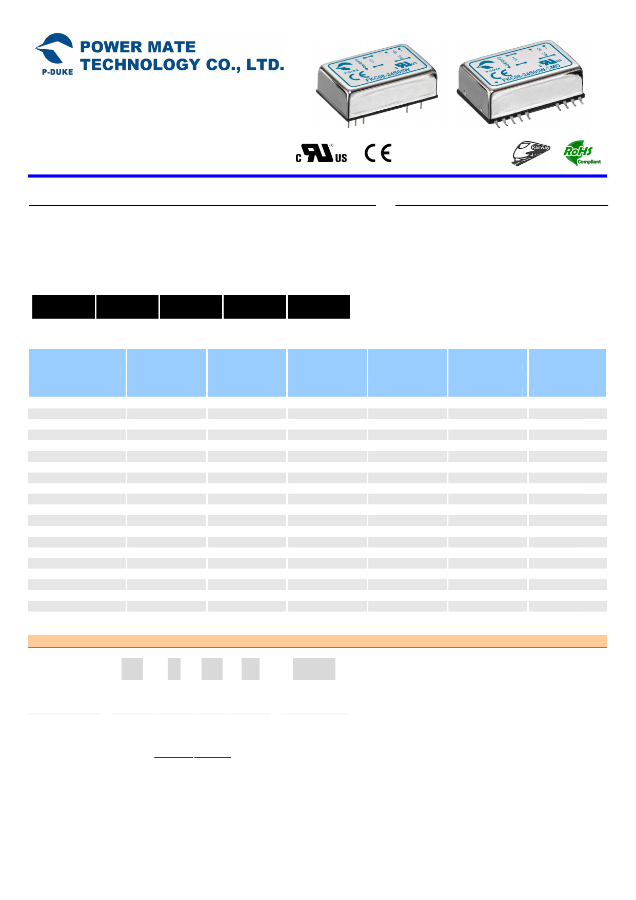
The FKC08W series offer 8 watts of output power from a package in an IC
compatible 24pin DIP configuration. FKC08W series have 4:1 ultra wide input
voltage of 9-36, 18-75VDC. The FKC08W have features 1600VDC of isolation,
short circuit protection and as well as five sided shielding.
T E C H N I C A L S P E C I F I C A T I O N All specifications are typical at nominal input, full load and 25ºC otherwise noted
OUTPUT SPECIFICATIONS
INPUT SPECIFICATIONS
Output power
Voltage accuracy
Full load and nominal Vin
8 Watts, max. Input voltage range
± 1%
24V nominal input
48V nominal input
9 – 36VDC
18 – 75VDC
Minimum load
0% Input filter
Pi type
Line regulation
LL to HL at Full Load
± 0.2% Input surge voltage
24V input
100mS max
48V input
Load regulation
Single (DIP)
No Load to Full Load Single (SMD)
± 0.5% Input reflected ripple current
± 1%
Nominal Vin and full load
Dual (SMD,DIP)
± 1% Start up time
Nominal Vin and
constant resistive load
Power up
Cross regulation (Dual) Asymmetrical load 25% / 100% FL
Ripple and noise
20MHz bandwidth
± 5%
See table Start-up voltage
24V input
48V input
50VDC
100VDC
20mAp-p
450mS, typ.
9VDC
18VDC
Temperature coefficient
Transient response recovery time
±0.02% / ºC, max.
25% load step change
250μS
Shutdown voltage
24V input
48V input
Remote ON/OFF (Note 6)
8VDC
16VDC
3.3V output
3.9VDC
DC-DC ON
Open or 3.0V < Vr < 12V
Over voltage protection 5.0V output
6.2VDC
DC-DC OFF
Short or 0V < Vr < 1.2V
(only single)
12V output
15V output
15VDC
18VDC
Input current of Remote control pin
Nominal Vin
-0.5mA ~ 0.5mA
Over load protection % of FL at nominal input
150%, typ. Remote off state input current
Nominal Vin
2.5mA
Short circuit protection
Continuous, automatics recovery ENVIRONMENTAL SPECIFICATIONS
GENERAL SPECIFICATIONS
Operating ambient
Vo:5V,12V,15V
±12V,±15V
-40ºC to +81ºC (without derating)
+81ºC to +105ºC (with derating)
Efficiency
Input to Output
See table temperature
1600VDC, min.
Vo:3.3V;±5V
-40ºC to +74ºC (without derating)
+74ºC to +105ºC (with derating)
Isolation voltage Input(Output) to Case DIP
SMD
1600VDC, min. Maximum case temperature
1000VDC, min.
+105ºC
Isolation resistance
109ohms, min. Storage temperature range
-55ºC to +125ºC
Isolation capacitance
1500pF, max. Thermal impedance
Nature convection
20ºC/Watt
Switching frequency
Approvals and standard
Case material
Base material
Potting material
300KHz, typ. Thermal shock
IEC60950-1, UL60950-1, EN60950-1
Vibration
Nickel-coated copper
Non-conductive black plastic Relative humidity
Epoxy (UL94-V0) EMC CHARACTERISTICS
MIL-STD-810F
MIL-STD-810F
5% to 95% RH
Dimensions
Weight
MTBF (Note 1)
1.25 X 0.80 X 0.40 Inch EMI (Note 7)
(31.8 X 20.3 X 10.2 mm)
BELLCORE-TR-NWT-000332
MIL-HDBK-217F
18g (0.62oz) ESD
2.350 x 10⁶ hrs
1.078 x 10⁶ hrs Radiated immunity
EN55022
EN61000-4-2
EN61000-4-3
Air
Contact
± 8KV
± 6KV
10 V/m
Class A
Perf. Criteria B
Perf. Criteria A
Fast transient (Note 8) EN61000-4-4
± 2KV Perf. Criteria A
Surge (Note 8)
EN61000-4-5
± 1KV Perf. Criteria A
Conducted immunity EN61000-4-6
10 Vr.m.s Perf. Criteria A
Page 1 of 3 Issued Date:2008/05/21
Share Link: 