NTE825 Просмотр технического описания (PDF) - NTE Electronics
Номер в каталоге
Компоненты Описание
производитель
NTE825 Datasheet PDF : 3 Pages
| |||
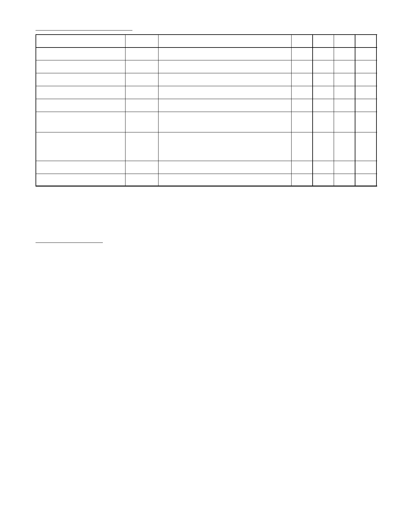
Electrical Characteristics: (TA = 25°C unless otherwise specified)
Parameter
Symbol
Test Conditions
Min Typ Max Unit
Operating Supply Voltage
Quiescent Current
Output Power
Voltage Gain
Bandwidth
Total Harmonic Distortion
VS
4–
IQ VS = 6V, RL = 4Ω, THD = 10%, Note 2 – 10
POUT VS = 6V, RL = 4Ω, THD = 10%, Note 2 0.8 1.0
AV VS = 6V, f = 1kHz 10µF from Pin2 to Pin6 23 26
BW VS = 6V, Pin2 and Pin6 Open
– 46
THD VS = 6V, RL = 4Ω, POUT = 500mW,
f = 1kHz, Pin2 and Pin6 Open
– 0.2
9V
20 mA
–W
30 dB
– kHz
1%
Power Supply Rejection PSRR VS = 6V, f = 1kHz, CBYPASS = 10µF,
– 50 – dB
Ratio
Pin2 and Pin6 Open, Referred to Output,
Note 3
Input Resistance
Input Bias Current
RIN
IBIAS
VS = 6V, Pins 7 and 8 Open
10 50 – kΩ
– 250 – mA
Note 2. If oscillation exists under some load conditions, add a 2.7Ω and 0.05µF series network from
Pin13 to GND.
Note 3. If load and bypass capacitor are returned to VS rather than GND, PSRR is typically 30dB.
Application Hints:
Gain Control
To make the NTE825 a more versatile amplifier, two pins (Pin2 and Pin6) are provided for gain
control. With Pin2 and Pin6 open, the gain is 20 (26dB). If a capacitor is put from Pin2 to Pin6,
the gain will go up to 200 (46dB). If a resistor is placed in series with the capacitor, the gain
can be set to any value from 20 to 200. A 10µf Electrolytic with positive to Pin6 is a usual value.
Additional external components can be placed in parallel with the internal feedback resistors
to tailor the gain and frequency response for inidividual applications. For example, a series
RC from Pin6 to Pin13 (paralleling the internal 15kΩ resistor) yields 6dB effective bass boost
if R ≅ 15kΩ and Pin2 is open. If Pin2 and Pin6 are bypassed, then R as low as 2kΩ can be
used. This restriction is because the amplifier is only compensated for closed–loop gains
greater than 9V/V.
Input Biasing
When using NTE825 with higher gains (bypassing the internal 1.35kΩ resistor between Pin2
and Pin6) it is necessary to bypass the unused input, preventing degradation of gain and pos-
sible instabilities. This is done with a 0.1µF capacitor or a short to GND depending on the DC
source resistance on the driven input.
Share Link: 