SZMMSZ5246BT3G Просмотр технического описания (PDF) - ON Semiconductor
Номер в каталоге
Компоненты Описание
производитель
SZMMSZ5246BT3G Datasheet PDF : 7 Pages
| |||
MMSZ52xxxT1G Series,
SZMMSZ52xxxT1G Series
Zener Voltage Regulators
500 mW SOD−123 Surface Mount
Three complete series of Zener diodes are offered in the convenient,
surface mount plastic SOD−123 package. These devices provide a
convenient alternative to the leadless 34−package style.
Features
• 500 mW Rating on FR−4 or FR−5 Board
• Wide Zener Reverse Voltage Range − 2.4 V to 110 V
• Package Designed for Optimal Automated Board Assembly
• Small Package Size for High Density Applications
• General Purpose, Medium Current
• ESD Rating of Class 3 (> 16 kV) per Human Body Model
• SZ Prefix for Automotive and Other Applications Requiring Unique
Site and Control Change Requirements; AEC−Q101 Qualified and
PPAP Capable
• These are Pb−Free Devices*
Mechanical Characteristics:
CASE: Void-free, transfer-molded, thermosetting plastic case
FINISH: Corrosion resistant finish, easily solderable
MAXIMUM CASE TEMPERATURE FOR SOLDERING PURPOSES:
260°C for 10 Seconds
POLARITY: Cathode indicated by polarity band
FLAMMABILITY RATING: UL 94 V−0
MAXIMUM RATINGS
Rating
Symbol
Max
Units
Total Power Dissipation on FR−5 Board,
PD
(Note 1) @ TL = 75°C
Derated above 75°C
500
mW
6.7
mW/°C
Thermal Resistance, Junction−to−Ambient RqJA
(Note 2)
340
°C/W
Thermal Resistance, Junction−to−Lead
(Note 2)
RqJL
150
°C/W
Junction and Storage Temperature Range TJ, Tstg −55 to +150 °C
Stresses exceeding Maximum Ratings may damage the device. Maximum
Ratings are stress ratings only. Functional operation above the Recommended
Operating Conditions is not implied. Extended exposure to stresses above the
Recommended Operating Conditions may affect device reliability.
1. FR−5 = 3.5 X 1.5 inches, using the minimum recommended footprint.
2. Thermal Resistance measurement obtained via infrared Scan Method.
*For additional information on our Pb−Free strategy and soldering details, please
download the ON Semiconductor Soldering and Mounting Techniques
Reference Manual, SOLDERRM/D.
© Semiconductor Components Industries, LLC, 2012
1
October, 2012 − Rev. 12
http://onsemi.com
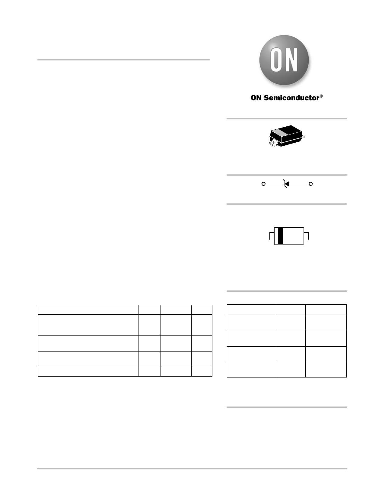
SOD−123
CASE 425
STYLE 1
1
Cathode
2
Anode
MARKING DIAGRAM
xx MG
1
G
xx = Device Code (Refer to page 3)
M = Date Code
G = Pb−Free Package
(Note: Microdot may be in either location)
ORDERING INFORMATION
Device
Package
Shipping†
MMSZ52xxBT1G, SOD−123
SZMMSZ52xxBT1G (Pb−Free)
3,000 /
Tape & Reel
MMSZ52xxCT1G, SOD−123
SZMMSZ52xxCT1G (Pb−Free)
3,000 /
Tape & Reel
MMSZ52xxBT3G, SOD−123
SZMMSZ52xxBT3G (Pb−Free)
10,000 /
Tape & Reel
MMSZ52xxCT3G, SOD−123
SZMMSZ52xxCT3G (Pb−Free)
10,000 /
Tape & Reel
†For information on tape and reel specifications,
including part orientation and tape sizes, please
refer to our Tape and Reel Packaging Specifications
Brochure, BRD8011/D.
DEVICE MARKING INFORMATION
See specific marking information in the device marking
column of the Electrical Characteristics table on page 3 of
this data sheet.
Publication Order Number:
MMSZ5221BT1/D
Share Link: 