LC82101 Просмотр технического описания (PDF) - SANYO -> Panasonic
Номер в каталоге
Компоненты Описание
производитель
LC82101 Datasheet PDF : 5 Pages
| |||
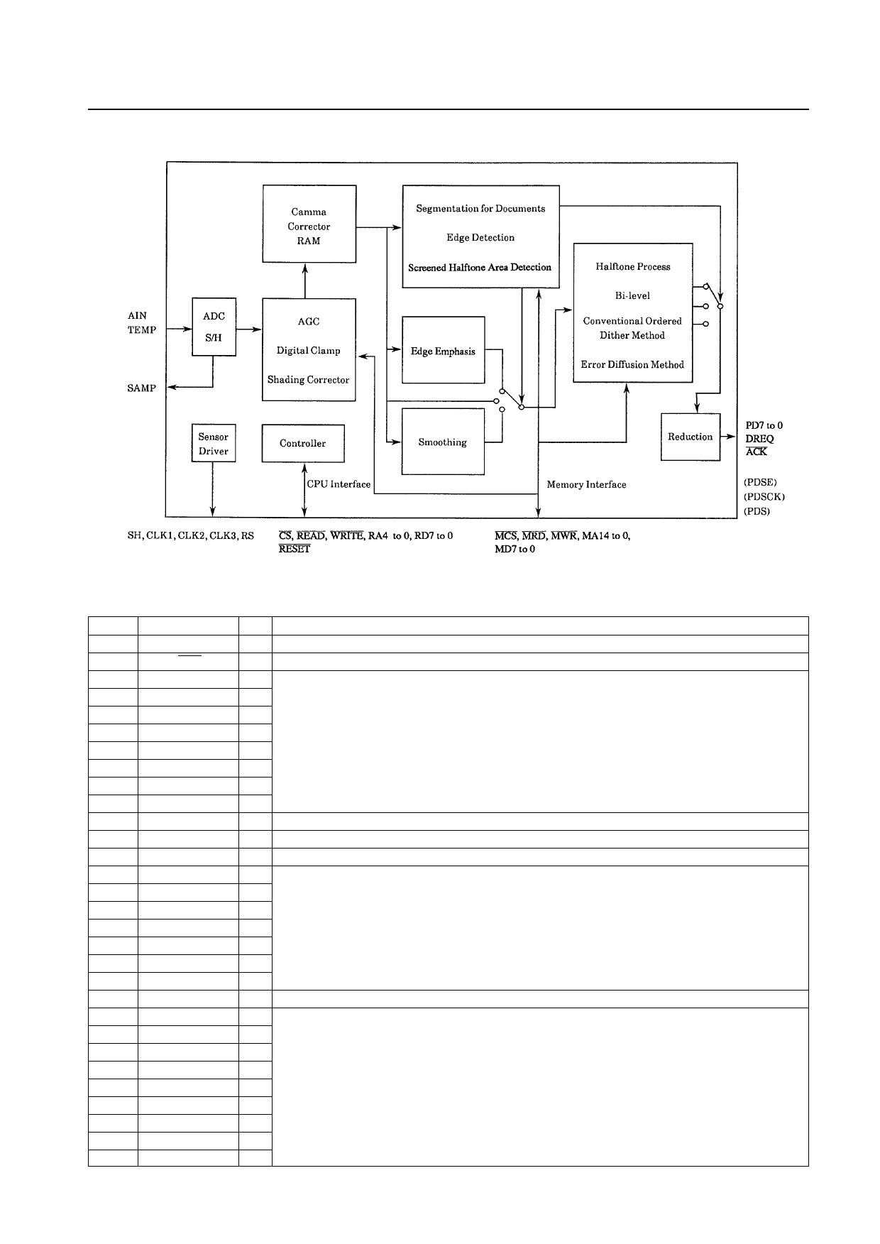
Block Diagram
LC82101
Pin Functions
Pin No.
1
2
3
4
5
6
7
8
9
10
11
12
13
14
15
16
17
18
19
20
21
22
23
24
25
26
27
28
29
30
Symbol
DREQ
ACK
PD0
PD1
PD2
PD3
PD4
PD5/SDE
PD6/SDCK
PD7/SD
MD0
DVDD
DGND
MD1
MD2
MD3
MD4
MD5
MD6
MD7
DGND
MA0
MA1
MA2
MA3
MA4
MA5
MA6
MA7
MA8
Type: I: Input pin, O: Output pin, B: Bidirectional pin, P: Power supply pin, NC: No connection
I/O
Function
O DMA data request signal output
I DMA acknowledge signal input
O
O Binary image data parallel data bus
O The data order is set by the MSBF register.
O
O
O Pin 8 can be switched to function as the serial data output valid period signal.
O Pin 9 can be switched to function as the serial data transfer clock.
O Pin 10 can be switched to function as the serial data output.
B External memory data bus
P Digital system power supply
P Digital system ground
B
B
B
B
External memory data bus
MD7 is the MSB and MD0 is the LSB.
B
B
B
P Digital system ground
O
O
O
O
O
External memory address
MA14 is the MSB and MA0 is the LSB.
O
O
O
O
Continued on next page.
No. 4982-2/5
Share Link: 