AD6402 Просмотр технического описания (PDF) - Analog Devices
Номер в каталоге
Компоненты Описание
производитель
AD6402 Datasheet PDF : 8 Pages
| |||
AD6402
VRF
C44
100nF
IFVCC1
C71
1nF
IFVCC2
RSSI
R8
4.7kΩ
C4
3.3nF
RSSI
IFIN
1
C69
2
1nF
3
10
9
L7
100nH
8
AD6402
C10
1nF
IFIN
DOUT
R30
2kΩ
C12
DFILP 33pF
RXBB
C58 R35
47pF 4.7kΩ
L5
150nH
4
7
5 B4535 6
L6
150nH
12pF
IFGND
R10
R9
PLLOUT 2kΩ
1kΩ
VCC C44
1nF
VIF
C43
VBAT
VREG
REG
PLLVCC
PLLGND
REXT
VRF
C11
100pF
R17
10kΩ
C14
68pF
100nF
CFILT
OBSOLETE VTUNE
C25
1nF
R26 C42
C41
1.2kΩ 47pF
8pF
C50
4.7nF
D3
D2
SMV
1204-37
L11
39nH
SMV
1204-36
R21
240Ω
VREF
IFC2
IFC1
IFC0
TXIF+
TXIF–
SLREF REF
VCO
VCOGND
CTL3
CTL2
CTL1
C28
1nF
TXOUT
TXOUTB
C29
1nF
C30
150pF
R16
330Ω
CP
COFF
C45 R22
131nF 330Ω
C32
REFIN 100nF
/3,/5
CP PD CP
C13
REFSEL
1nF
C31
R70
FMMOD2
R28
330Ω
R32
330Ω
MODOUT
FMMOD1
C52
100pF
C51
180pF
RCLK
TXBB
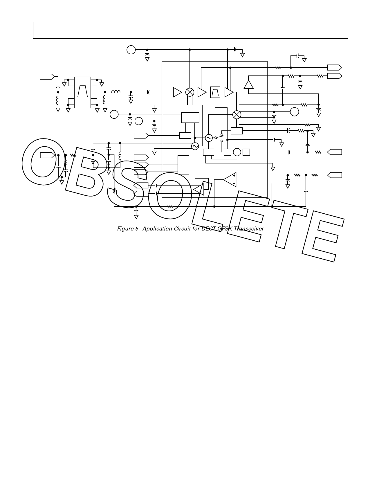
Figure 5. Application Circuit for DECT GFSK Transceiver
supply current levels when not allocated to an active transmit or transfer characteristic of the loop filter and hence the lock time,
receive timeslot in a TDMA system.. The respective transmit
settling time and bandwidth of the loop. REXT should use the
and receive blocks can be turned on only as needed thereby
recommended value as shown.
reducing power consumption and extending battery life of
handheld terminals.
Finally, the demodulator is followed by a voltage follower,
which is configured as a data filter. This data filter is used to
The component selection in Figure 5 is explained as follows:
bandlimit the FM noise generated in the demodulator. It also
The IF input is driven from the output of a SAW filter via an
attenuates undesired adjacent channel interferers. The compo-
impedance matching circuit as shown. This matching minimizes nent values chosen will be a trade-off between the amount of
the insertion loss of the filter and follows the filter manufactur- band limiting required and attenuation of the in-band desired
ers recommendations. The tank circuit shown uses two varactor signal.
diodes. One diode (D3) is biased by the output of the IF PLL
loop filter and ensures that the IF VCO frequency is correctly
centered. The second diode is provided to enable a modulation
signal, which is generated at the output of the on-chip op amp
(MODOUT), to be coupled into the VCO tank and thereby
DECT Application Circuit Notes (Figure 5)
1. Signal Description
VRF: Regulated Supply Voltage; Nominal Value 2.85 V.
VCC: Unregulated battery voltage; 3.1 V–4.5 V
implement a modulation of the VCO frequency. In the case of
VTUNE: Synthesizer Control Voltage; Range dependent on
DECT, the IF VCO control loop is opened while the VCO is
loop filter and synth charge pump compliance.
being modulated by the transmit bit stream. The loop is opened
by tri-stating the output of the IF VCO PLL charge pump.
TXBB: Baseband transmit modulation voltage; typically
SLREF ± 0.7 V
The exact component values used around the modulation am-
plifier will be determined by the amount of attenuation required
for suppression of baseband transmit spurii and images. These
artifacts are usually present if the baseband FSK signal is gener-
RCLK: Reference clock for PLL demodulator; 13.824 MHz
(2nd IF frequency = (N/M) × Frclk where N = 3 or 5, and
M = 2. Maximum 2nd IF = c.26 MHz)
ated by a ROMDAC. In most instances a second or third order 2. Typical IF input sensitivity referred to the input of SAW
Bessel or Butterworth filter will be required.
filter for the above application will be –72 dBm.
A capacitor to ground is required to be connected to COFF.
This capacitor stores the demodulator charge-pump voltage
required to lock the demodulator VCO to the reference fre-
quency. The dynamic response of the demodulator loop is con-
trolled by selection of the values for C45 and R22 which are
connected in series to CFILT. These components determine the
3. TxBB filter is user configurable. In the above application, the
filter is implemented to remove images generated by ROM
DAC baseband signal generators. Other implementations are
possible including passive pulse shaping circuits which elimi-
nate the need for such filtering.
REV. 0
–7–
Share Link: 