AD9870 Просмотр технического описания (PDF) - Analog Devices
Номер в каталоге
Компоненты Описание
производитель
AD9870 Datasheet PDF : 20 Pages
| |||
AD9870
PC
PE
WRITE OPERATION:
PD
A5
A0
D7
D6
D0
READ OPERATION:
PD
A5
A0
D7
D6
D0
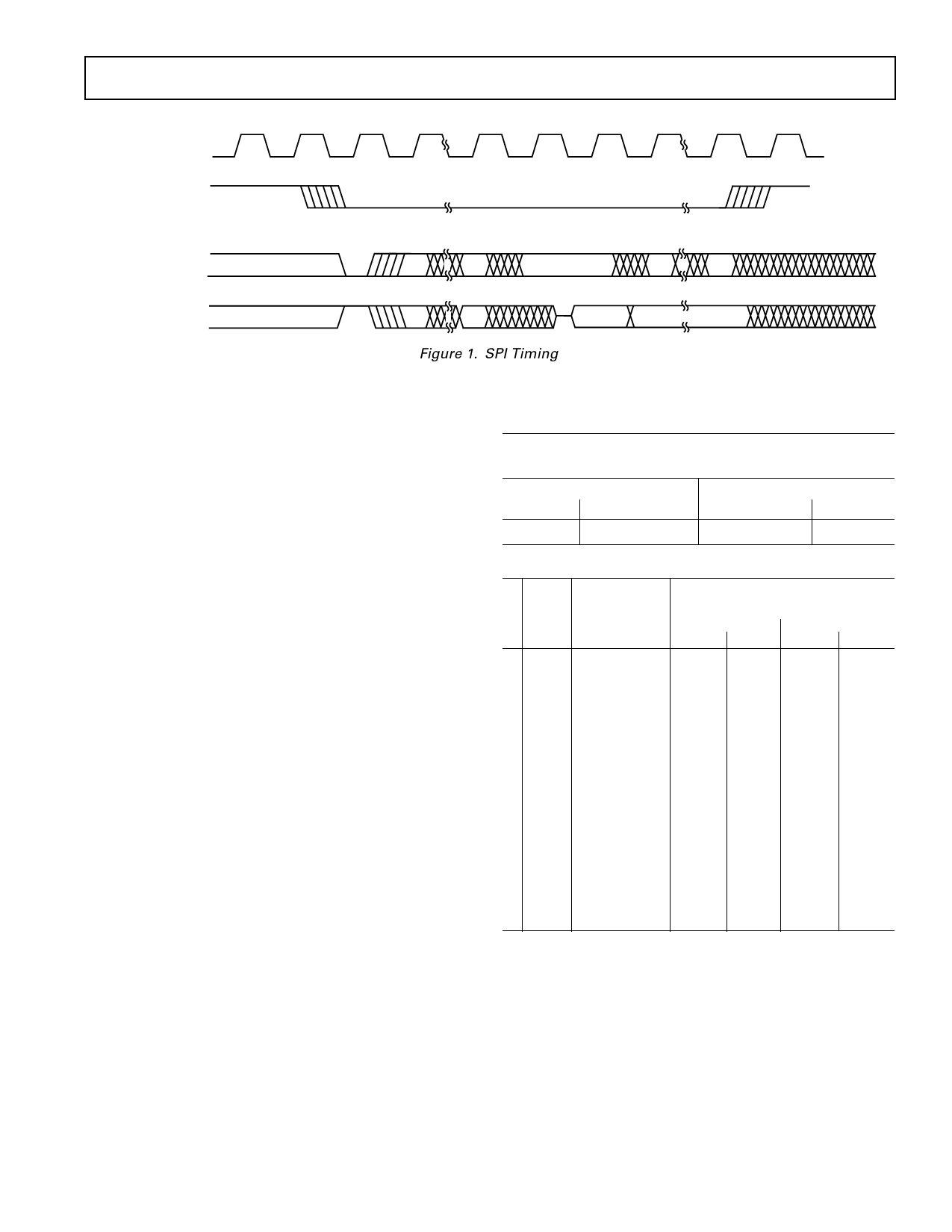
Figure 1. SPI Timing
Figure 1 illustrates the timing for the SPI port. After the periph-
eral enable (PE) signal goes low, data (PD) is read on the rising
edges of the clock (PC). The first bit is a read/not-write indica-
tor; the next six bits are address bits; the eighth bit is ignored;
the last eight bits are data. Address and data are given MSB first.
If the read/not-write indicator is a zero, a write operation occurs
and the data bits are shifted in. If the read/not-write indicator is
a one and if the read-back enable bit (Reg. 3A, Bit 3) has been
set, a read operation occurs and data is shifted out the data pin on
the falling edges of the clock. PE stays low during the operation
and goes high at the end of the transfer. If PE rises before an addi-
tional eight clock cycles have passed, the operation is aborted.
If PE stays low for an additional eight clock cycles, the destina-
tion address is incremented and another eight bits of data are
shifted in. Again, should PE rise early, the current byte is ignored.
By using this implicit addressing mode, the entire chip can be
configured with a single write operation. Registers identified as
being subject to frequent updates, namely those associated with
power control and AGC operation, have been assigned adjacent
addresses to minimize the time required to update them. The auto-
increment mode is not supported for read operations.
Multibyte registers are “big-endian” (the most significant byte
has the lower address) and are updated when a write to the least
significant byte occurs.
SYNCHRONOUS SERIAL INTERFACE (SSI)
The primary output of the AD9870 is the converted signal, which
is available from the SSI port as a serial bit stream. The bit stream
consists of a 16-bit I word followed by a 16-bit Q word, where
each word is given MSB first and is in two’s-complement form.
AGC, signal strength, and synchronization information may also
be embedded in the data stream. The output bit rate (fCLKOUT)
is equal to the modulator clock frequency (fCLK) divided by
the contents of the SSIORD register. Users must verify that the
output bit rate is sufficient to accommodate the required num-
ber of bits per frame (see Table II) and that the chosen output
rate does not introduce harmful spurs. Idle (high) bits are used
to fill out each frame; the frame lengths listed in Table II
assume that with embedded frame sync (EFS = 1), at least 10
idle bits are desired.
Table II. Max Legal SSIORD Values for 16-Bit I/O Data and
Decimation by 60 n
Bits per Sample
(Min No. of Bits per Frame)
EAGC = 0
EFS =1
EFS = 0
32
49
EAGC = 1
EFS = 0
EFS = 1
48/40*
69/59*
Output
Sample Rate Max SSIORD Setting (Decimal)
Dec’n (kSPS, for
EAGC = 0
EAGC = 1
M Factor fCLK = 18 MHz) EFS = 0 EFS = 1 EFS = 0 EFS = 1
0 60
1 120
2 180
3 240
4 300
5 360
6 420
7 480
8 540
9 600
10 660
11 720
12 780
13 840
14 900
15 960
300
150
100
75
60
50
42.857
37.5
33.333
30
27.272
25
23.077
21.428
20
18.75
1
1
1
1
3
2
2
1
5
3
3
2
7
4
5
3
9
5
6
4
11
7
7
5
13
8
8
5
14
9
10
6
15
10
11
7
15
11
12
8
15
13
13
9
15
14
14
10
15
15
15
11
15
15
15
11
15
15
15
12
15
15
15
13
*If the AAGC Bit of SSICRA is set.
Figure 2 illustrates the output timing of the SSI port for several
SSI control register settings. In the default mode of operation,
data is shifted out on rising edges of CLKOUT after a pulse is
output from the frame sync (FS) pin. As described above, the
output data consists of a 16-bit I sample followed by a 16-bit
Q sample plus two optional bytes containing AGC and status
information.
REV. 0
–7–
Share Link: 