M4A5-32/32-7VI –ü—Ä–ĺ—Ā–ľ–ĺ—ā—Ä —ā–Ķ—Ö–Ĺ–ł—á–Ķ—Ā–ļ–ĺ–≥–ĺ –ĺ–Ņ–ł—Ā–į–Ĺ–ł—Ź (PDF) - Lattice Semiconductor
–Ě–ĺ–ľ–Ķ—Ä –≤ –ļ–į—ā–į–Ľ–ĺ–≥–Ķ
–ö–ĺ–ľ–Ņ–ĺ–Ĺ–Ķ–Ĺ—ā—č –ě–Ņ–ł—Ā–į–Ĺ–ł–Ķ
–Ņ—Ä–ĺ–ł–∑–≤–ĺ–ī–ł—ā–Ķ–Ľ—Ć
M4A5-32/32-7VI Datasheet PDF : 63 Pages
| |||
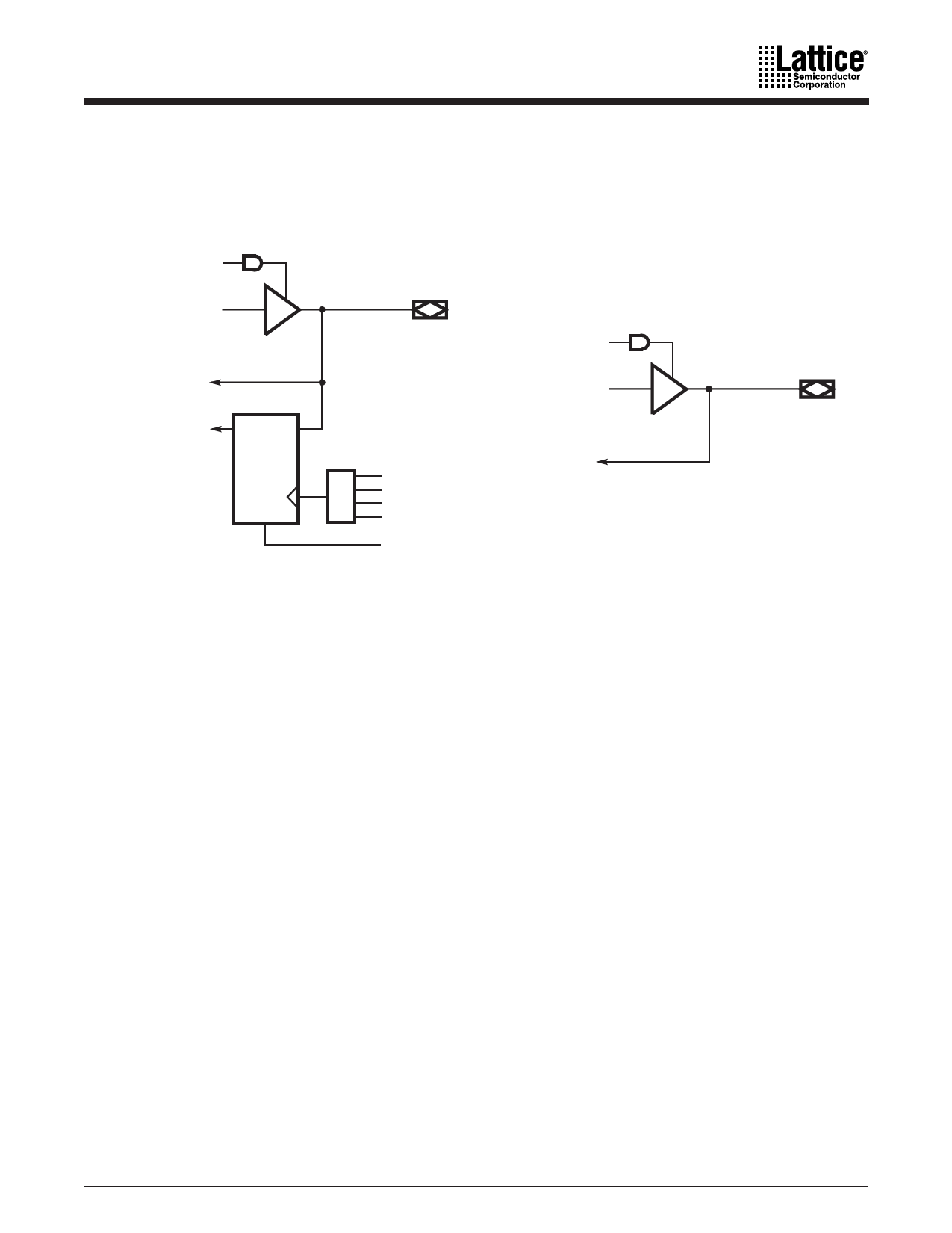
I/O Cell
The I/O cell (Figures 10 and 11) simply consists of a programmable output enable, a feedback path, and
flip-flop (except ispMACH 4A devices with 1:1 macrocell-I/O cell ratio). An individual output enable
product term is provided for each I/O cell. The feedback signal drives the input switch matrix.
Individual
Output Enable
Product Term
From Output
Switch Matrix
To Input
Switch
Matrix
Q D/L
Block CLK0
Block CLK1
Block CLK2
Block CLK3
Power-up reset
17466G-017
Figure 10. I/O Cell for ispMACH 4A Devices with 2:1
Macrocell-I/O Cell Ratio
Individual
Output Enable
Product Term
From Output
Switch Matrix
To Input
Switch
Matrix
17466G-018
Figure 11. I/O Cell for ispMACH 4A Devices with 1:1
Macrocell-I/O Cell Ratio
The I/O cell (Figure 10) contains a flip-flop, which provides the capability for storing the input in a D-type
register or latch. The clock can be any of the PAL block clocks. Both the direct and registered versions of
the input are sent to the input switch matrix. This allows for such functions as ‚Äútime-domain-multiplexed‚ÄĚ
data comparison, where the first data value is stored, and then the second data value is put on the I/O pin
and compared with the previous stored value.
Note that the flip-flop used in the ispMACH 4A I/O cell is independent of the flip-flops in the macrocells.
It powers up to a logic low.
Zero-Hold-Time Input Register
The ispMACH 4A devices have a zero-hold-time (ZHT) fuse which controls the time delay associated with
loading data into all I/O cell registers and latches. When programmed, the ZHT fuse increases the data path
setup delays to input storage elements, matching equivalent delays in the clock path. When the fuse is erased,
the setup time to the input storage element is minimized. This feature facilitates doing worst-case designs
for which data is loaded from sources which have low (or zero) minimum output propagation delays from
clock edges.
ispMACH 4A Family
17
Share Link: 