LC75878W(2013) Просмотр технического описания (PDF) - ON Semiconductor
Номер в каталоге
Компоненты Описание
производитель
LC75878W Datasheet PDF : 35 Pages
| |||
LC75878W
Specifications
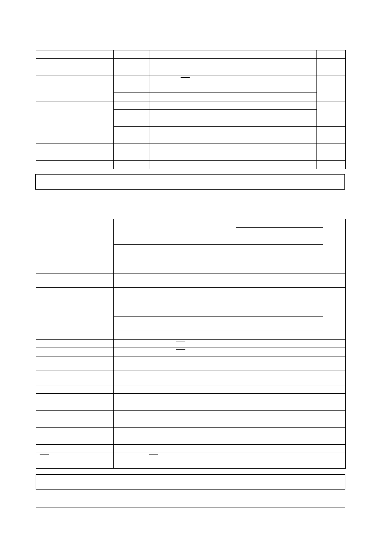
Absolute Maximum Ratings at Ta = 25°C, VSS = 0V
Parameter
Maximum supply voltage
Input voltage
Output voltage
Output current
Allowable power dissipation
Symbol
VDD max
VLCD max
VIN1
VIN2
VIN3
VOUT1
VOUT2
IOUT1
IOUT2
IOUT3
Pd max
Conditions
VDD
VLCD
CE, CL, DI, INH
OSC
VLCD1, VLCD2, VLCD3, VLCD4
OSC, P1 to P4
VLCD0, S1 to S75, COM1 to COM10
S1 to S75
COM1 to COM10
P1 to P4
Ta=85°C
Operating temperature
Storage temperature
Topr
Tstg
Ratings
Unit
-0.3 to +7.0
V
-0.3 to +12.0
-0.3 to +7.0
-0.3 to VDD+0.3
V
-0.3 to VLCD+0.3
-0.3 to VDD+0.3
V
-0.3 to VLCD+0.3
300
μA
3
mA
5
200
mW
-40 to +85
°C
-55 to +125
°C
Stresses exceeding Maximum Ratings may damage the device. Maximum Ratings are stress ratings only. Functional operation above the Recommended Operating
Conditions is not implied. Extended exposure to stresses above the Recommended Operating Conditions may affect device reliability.
Allowable Operating Ranges at Ta = -40 to +85°C, VSS = 0V
Parameter
Supply voltage
Output voltage
Symbol
VDD
VLCD
VLCD
VLCD0
Conditions
VDD
VLCD, When the display contrast adjustment
circuit is used
VLCD, When the display contrast adjustment
circuit is not used
VLCD0
Input voltage
VLCD1
VLCD1
VLCD2
VLCD2
VLCD3
VLCD3
Input high level voltage
Input low level voltage
Recommended external resistance
Recommended external
capacitance
Guaranteed oscillation range
Data setup time
Data hold time
CE wait time
CE setup time
CE hold time
High level clock pulse width
Low level clock pulse width
INH switching time
VLCD4
VIH
VIL
ROSC
COSC
fOSC
tds
tdh
tcp
tcs
tch
tφH
tφL
tc
VLCD4
CE, CL, DI, INH
CE, CL, DI, INH
OSC
OSC
OSC
CL, DI
CL, DI
CE, CL
CE, CL
CE, CL
CL
CL
INH, CE
[Figure 2]
[Figure 2]
[Figure 2]
[Figure 2]
[Figure 2]
[Figure 2]
[Figure 2]
[Figure 3],[ Figure 4],[ Figure 5]
min
2.7
Ratings
typ
unit
max
6.0
7.0
11.0
V
4.5
11.0
VLCD4
+4.5
VLCD
V
3/4(VLCD0
-VLCD4)
VLCD0
2/4(VLCD0
-VLCD4)
VLCD0
V
1/4(VLCD0
-VLCD4)
VLCD0
0
1.5
0.8VDD
0
6.0
V
0.2VDD
V
43
kΩ
680
pF
25
50
100 kHz
160
ns
160
ns
160
ns
160
ns
160
ns
160
ns
160
ns
10
μs
No.6473-2/35
Share Link: 