LB11920-E Просмотр технического описания (PDF) - ON Semiconductor
Номер в каталоге
Компоненты Описание
производитель
LB11920-E Datasheet PDF : 10 Pages
| |||
LB11920
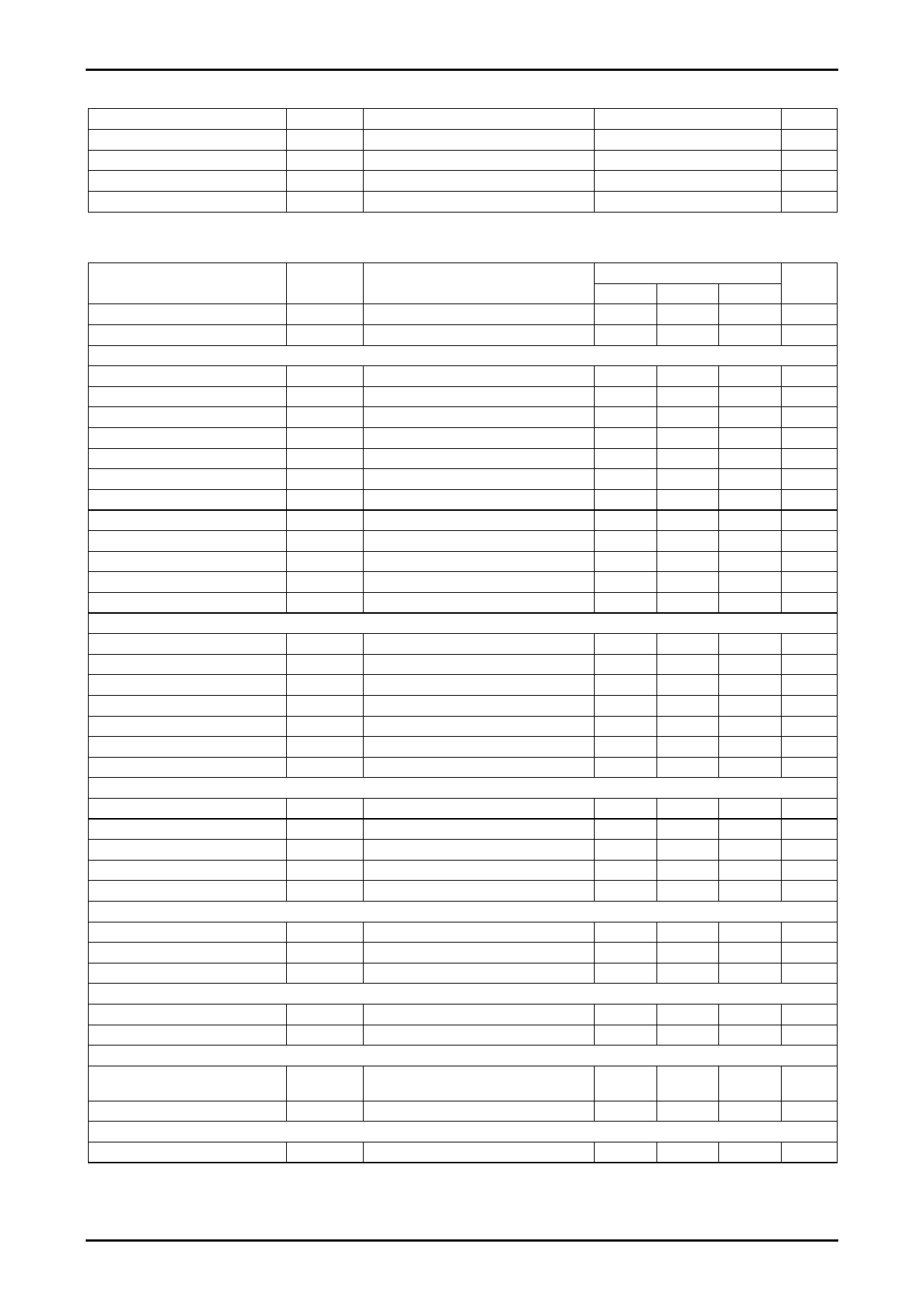
Allowable Operating Conditions at Ta = 25°C
Parameter
Supply voltage range 1
Supply voltage range 2
HP pin applied voltage
HP pin output current
Symbol
VM
VCC
VHP
IHP
Conditions
Ratings
Unit
9.5 to 30
V
4.5 to 5.5
V
0 to 32
V
0 to 3
mA
Electrical Characteristics at Ta = 25°C, VM = RF = 27V, VCC = 5V
Parameter
Symbol
Conditions
Supply current 1
Supply current 2
Output block
IVCC-1
IVCC-2
VCC pin
VCC pin at stop mode
Output saturation voltage 1
Output saturation voltage 2
Output saturation voltage 3
Output leakage current
Output delay time 1
VO sat1
VO sat2
VO sat3
IO leak
td1
IO = 1.0A, VO (sink) + VO (source)
IO = 2.0A, VO (sink) + VO (source)
IO = 3.0A, VO (sink) + VO (source)
PWMIN “H” → “L”
Output delay time 2
td2
PWMIN “L” → “H”
Lower diode forward 1
VD1-1
ID = -1.0A
Lower diode forward 2
VD1-2
ID = -2.0A
Lower diode forward 3
VD1-3
ID = -3.0A
Upper diode forward 1
VD2-1
ID = 1.0A
Upper diode forward 2
VD2-2
ID = 2.0A
Upper diode forward 3
VD2-3
ID = 3.0A
Hall Amplifier
Input bias current
IHB
Common-mode input voltage range 1 VICM1
Hall device used
Common-mode input voltage range 2 VICM2
For input one-side bias (Hall IC application)
Hall input sensitivity
at differential input
Hysteresis width
Input voltage low → high
ΔVIN
VSLH
Input voltage high → low
VSHL
PWM oscillator
Output H level voltage
Output L level voltage
External C charge current
VOH (PWM)
VOL (PWM)
ICHG(PWM)
VPWM = 2.1V
Oscillator frequency
f (PWM)
C = 1000pF
Amplitude
V (PWM)
CSD circuit
Operating voltage
External C charge current
VOH (CSD)
ICHG (CSD) VCSD = 0V
Operating time
T (CSD)
C = 10μF, Design target value*
HP pin
Output low level voltage
Output leakage current
VOL (HP)
Ileak(HP)
IHP = 2mA
VHP = 30V
Thermal shutdown operation
Thermal shutdown operating
temperature
Hysteresis width
TTSD
ΔTSD
Design target value* (junction temperature)
Design target value* (junction temperature)
Current limiter circuit (RF pin)
Limiter voltage
VRF
Note : * This parameter is a design target value and is not measured.
Ratings
Unit
min
typ
max
9
13
mA
2.0
3.0
mA
1.7
2.4
V
2.0
2.9
V
2.4
3.5
V
100
μA
1.25
2.5
μs
1.8
3.6
μs
1.1
1.5
V
1.3
1.9
V
1.5
2.3
V
1.3
1.7
V
2.0
2.7
V
2.7
3.7
V
-2
-0.1
μA
0.5
VCC-2.0
V
0
VCC
V
50
mVp-p
20
30
50
mV
5
15
25
mV
-25
-15
-5
mV
2.75
3.0
3.25
V
1.0
1.2
1.3
V
-60
-45
-30
μA
15.8
20
24.2 kHz
1.6
1.8
2.1 Vp-p
3.6
3.9
4.2
V
-15
-11
-7
μA
3.5
s
0.1
0.4
V
10
μA
150
180
°C
45
°C
0.45
0.5
0.55
V
Continued on next page.
No.7229-2/10
Share Link: 