CS5207A-1 Просмотр технического описания (PDF) - Cherry semiconductor
Номер в каталоге
Компоненты Описание
производитель
CS5207A-1 Datasheet PDF : 7 Pages
| |||
Absolute Maximum Ratings
Input Voltage...............................................................................................................................................................................6V
Operating Junction Temperature Range .........................................................................................................0¡C ² TJ ² 150¡C
Storage Temperature Range ..............................................................................................................................-65¡C to +150¡C
Lead Temperature Soldering
Wave Solder (through hole styles only)....................................................................................10 sec. max, 260¡C peak
ESD Damage Threshold ..........................................................................................................................................................2kV
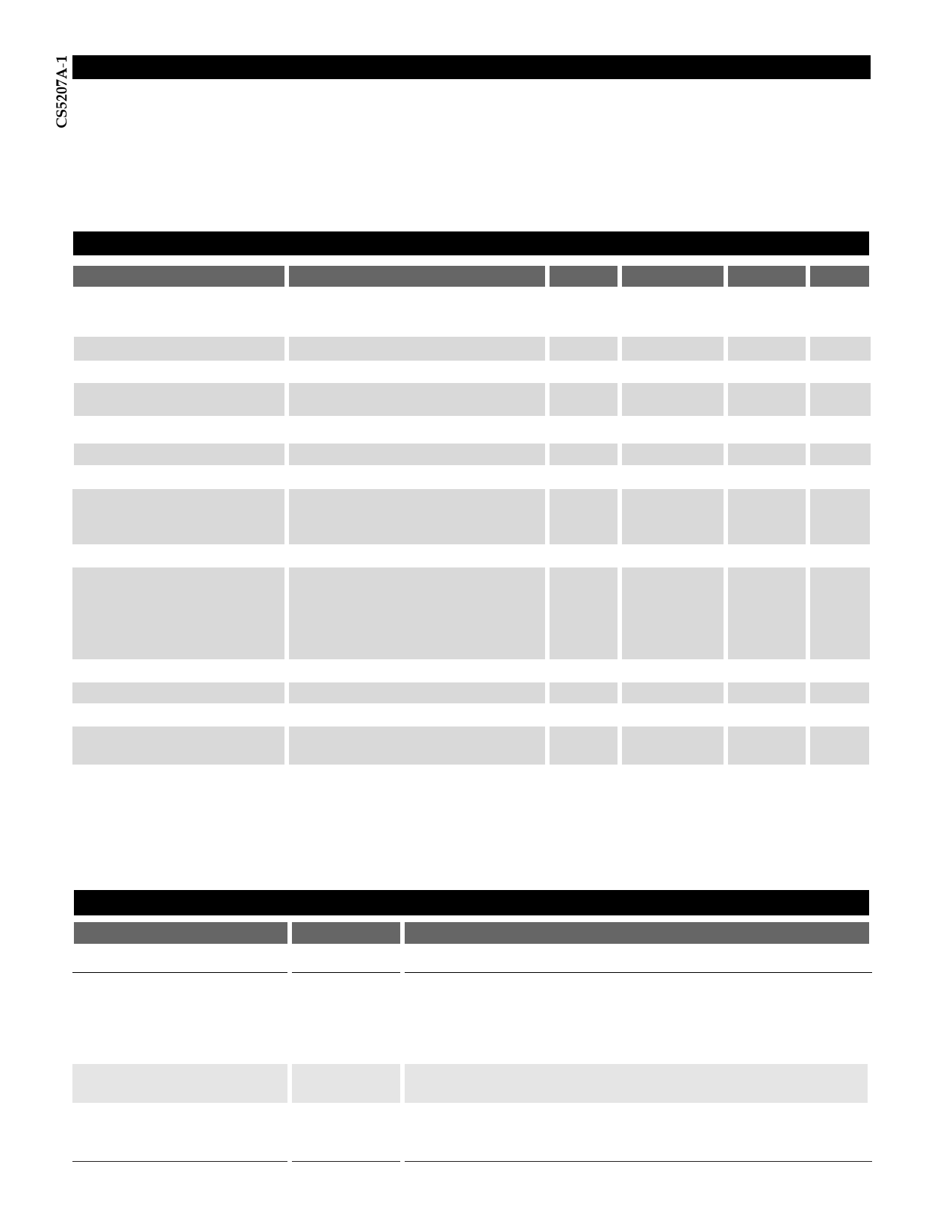
Electrical Characteristics: 0¡C²TA = 70¡C, 0¡C²TJ = 150¡C, VAdj = 0V unless otherwise specified.
PARAMETER
Reference voltage
Line Regulation
Load Regulation
Minimum Load Current
(Note 1)
Adjust Pin Current
Current Limit
Short Circuit Current
Ripple Rejection
(Note 2)
Thermal Regulation (Note 2)
Dropout Voltage
(Minimum VIN -VOUT)
(Note 3)
RMS Output Noise
Temperature Stability
Thermal Shutdown (Note 4)
Thermal Shutdown Hysteresis
(Note 4)
TEST CONDITIONS
VIN=2.75V to 5.5V, IOUT=10mA to 7A
VIN=2.75V to 5.5V, IOUT=10mA
VIN=2.75V,IOUT=10mA to 7A
VIN=5V, ÆVOUT=+1.5%
VIN=2.75V,IOUT=10mA
VIN=2.75V,ÆVOUT= -1.5%
VIN=2.75V,VOUT=0V
VIN=3.25V,
VRipple=1VP-P@120Hz,
IOUT=4A,CAdj=0.1µF; COUT = 22µF
30ms Pulse, TA=25¡C
IOUT=100mA
IOUT=1A
IOUT=2.75A
IOUT=4A
IOUT=7A
Freq=10Hz to 10kHz, TA=25¡C
MIN
1.234
(-1.5%)
7.1
5.0
60
150
TYP
1.253
.02
.04
5
70
8.0
9.0
80
0.002
0.92
0.93
0.94
0.95
0.96
0.003
0.5
180
25
MAX
1.271
(+1.5%)
.20
.50
10
UNIT
V
%
%
mA
120
µA
A
A
dB
%/W
1.15
V
1.15
V
1.15
V
1.15
V
1.25
V
%VOUT
%
210
¡C
¡C
Note 1:
Note 2:
Note 3:
Note 4:
The minimum load current is the minimum current required to maintain regulation. Normally the current in the resistor divider used to set
the output voltage is selected to meet the minimum load current requirement.
This parameter is guaranteed by design and is not 100% production tested.
Dropout voltage is defined as the minimum input/output voltage differential required to maintain 1.5% regulation.
This parameter is guaranteed by design, but not parametrically tested in production. However, a 100% thermal shutdown functional test is
performed on each part.
Package Pin Description
PACKAGE PIN #
3L TO-220
1
2
3
PIN SYMBOL
FUNCTION
Adjust
VOUT
VIN
This pin is connected to the low side of the internally trimmed 1.5%
bandgap reference voltage and carries a bias current of about 70µA.
A resistor divider from Adj to VOUT and from Adj to ground sets the
output voltage. Also, transient response can be improved by adding
a small bypass capacitor from this pin to ground.
This pin is connected to the emitter of the power pass transistor and
provides a regulated voltage capable of sourcing 7A of current.
This is the supply voltage for the regulator. For the device to regu-
late, this voltage should be between 1V and 1.25V (depending on the
output current) greater than the output voltage.
2
Share Link: 