CDP1823C/3 Просмотр технического описания (PDF) - Intersil
Номер в каталоге
Компоненты Описание
производитель
CDP1823C/3 Datasheet PDF : 6 Pages
| |||
CDP1823C/3
Read Cycle Dynamic Electrical Specifications tR, tF = 10ns, CL = 50pF (Continued)
LIMITS
PARAMETER
SYMBOL
VDD
(V)
+25oC, -55oC
MIN
MAX
+125oC
MIN
MAX
UNITS
Access Time from MRD (Note 1)
tAM
5
-
310
-
435
ns
Data Hold Time After Read
tDH
5
50
-
70
-
ns
NOTE:
1. Limits designate 100% testing. All other limits are designer’s parameters under given test conditions and do not represent 100% testing.
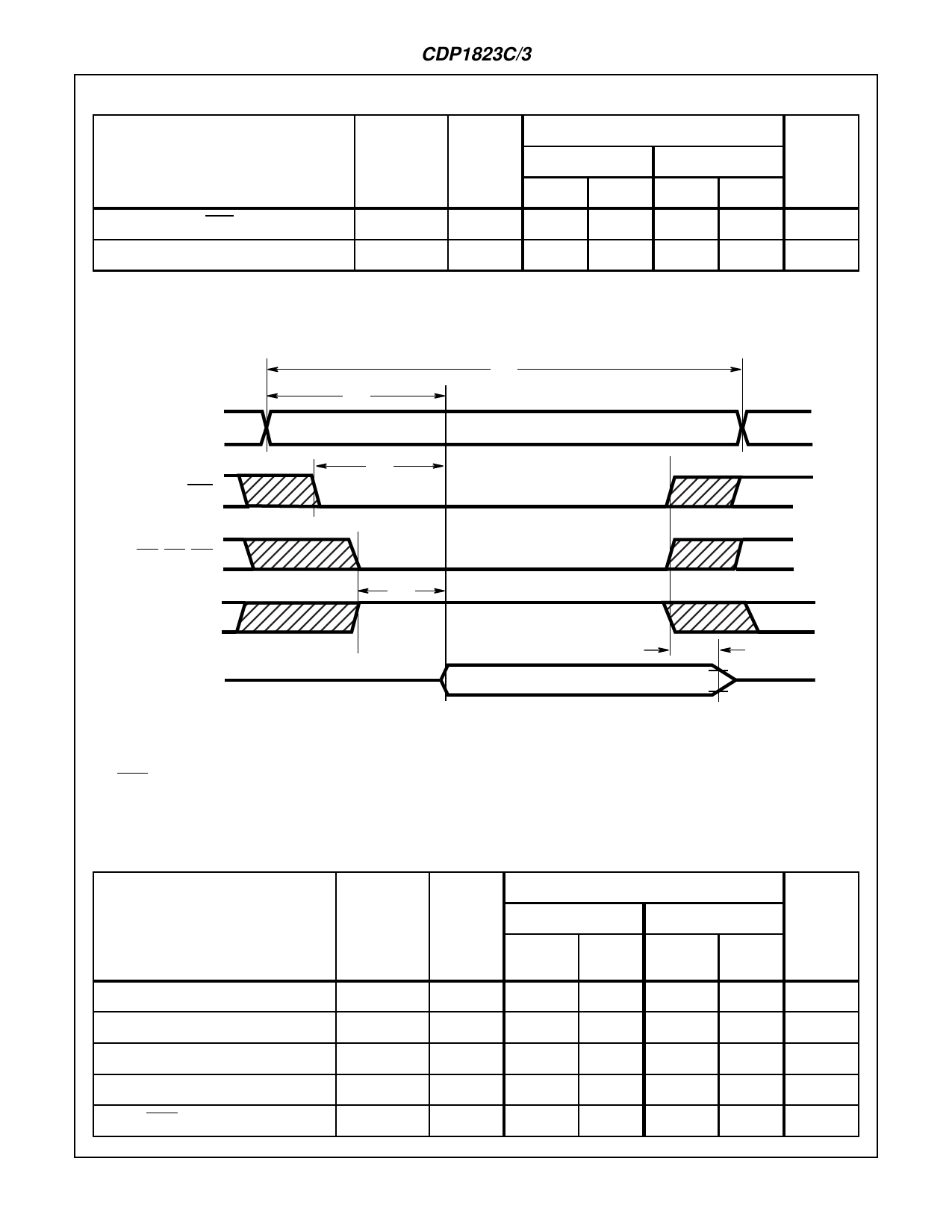
ADDRESS
MRD
tRC
tAA
tAM
(NOTE 1)
CS2, CS3, CS5
CS1, CS4
(NOTE 1)
tAC
HIGH IMPEDANCE
VALID DATA
tDH
90%
10%
NOTES:
1. Minimum timing for valid data output. Longer times will initiate an earlier but invalid output.
2. MWR is high during read operation. Timing measurement reference is 0.5VDD.
FIGURE 1. READ CYCLE TIMING DIAGRAM
Write Cycle Dynamic Electrical Specifications tR, tF = 10ns, CL = 50pF
LIMITS
+25oC, -55oC
+125oC
PARAMETER
SYMBOL
VDD
(V)
(NOTE 2)
MIN
MAX
(NOTE 2)
MIN
MAX
Write Cycle
Address Setup Time (Note 1)
Address Hold Time
Write Pulse Width (Note 1)
Data to MWR Setup Time (Note 1)
tWC
tAS
tAH
tWW
tDS
5
280
-
400
-
5
70
-
100
-
5
70
-
100
-
5
140
-
200
-
5
70
-
100
-
UNITS
ns
ns
ns
ns
ns
6-34
Share Link: 