SFT1341-W Просмотр технического описания (PDF) - ON Semiconductor
Номер в каталоге
Компоненты Описание
производитель
SFT1341-W Datasheet PDF : 6 Pages
| |||
Electrical Characteristics at Ta = 25°C
Parameter
Symbol
Drain to Source Breakdown Voltage
Zero-Gate Voltage Drain Current
Gate to Source Leakage Current
Gate Threshold Voltage
Forward Transconductance
Static Drain to Source On-State Resistance
Input Capacitance
Output Capacitance
Reverse Transfer Capacitance
Turn-ON Delay Time
Rise Time
Turn-OFF Delay Time
Fall Time
Total Gate Charge
Gate to Source Charge
Gate to Drain “Miller” Charge
Forward Diode Voltage
V(BR)DSS
IDSS
IGSS
VGS(th)
gFS
RDS(on)1
RDS(on)2
RDS(on)3
Ciss
Coss
Crss
td(on)
tr
td(off)
tf
Qg
Qgs
Qgd
VSD
SFT1341
Conditions
ID= –1mA, VGS=0V
VDS= –40V, VGS=0V
VGS=±8V, VDS=0V
VDS= –10V, ID= –1mA
VDS= –10V, ID= –5A
ID= –5A, VGS= –4.5V
ID= –5A, VGS= –2.5V
ID= –2.5A, VGS= –1.8V
VDS= –20V, f=1MHz
See specified Test Circuit.
VDS= –20V, VGS= –4.5V, ID= –10A
IS= –10A, VGS=0V
min
–40
Value
typ
–0.4
4.6
7.7
86
110
140
650
65
50
9.0
50
81
80
8.0
1.4
2.5
–1.0
Unit
max
V
–1 μA
±10 μA
–1.4 V
S
112 mΩ
154 mΩ
210 mΩ
pF
pF
pF
ns
ns
ns
ns
nC
nC
nC
–1.5 V
Product parametric performance is indicated in the Electrical Characteristics for the listed test conditions, unless otherwise noted. Product performance may not be
indicated by the Electrical Characteristics if operated under different conditions.
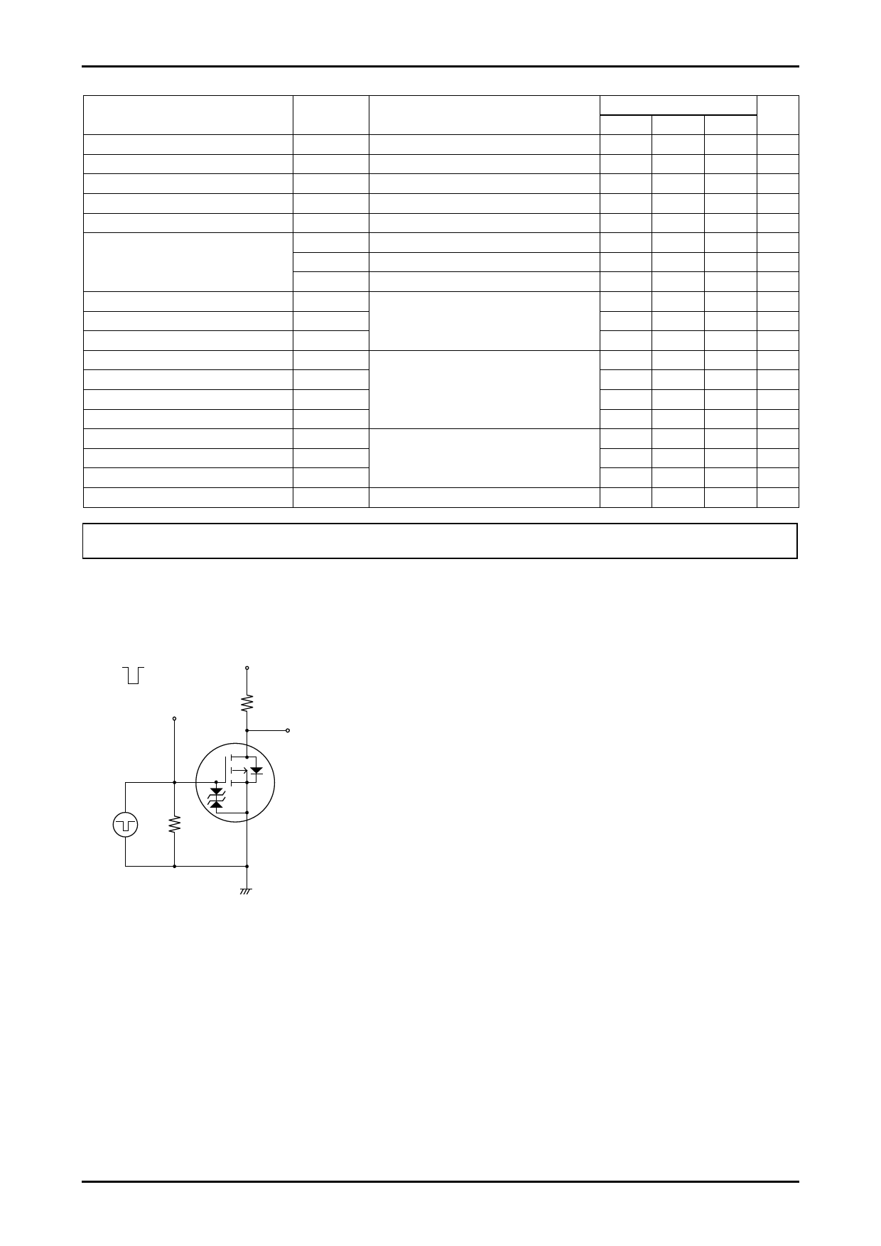
Switching Time Test Circuit
VIN
0V
--4.5V
VIN
PW=10μs
D.C.≤1%
G
VDD= --20V
ID= --5A
RL=4Ω
D
VOUT
SFT1341
P.G
50Ω
S
No.A1444-2/6
Share Link: 