RF2174PCBA-41X Просмотр технического описания (PDF) - RF Micro Devices
Номер в каталоге
Компоненты Описание
производитель
RF2174PCBA-41X Datasheet PDF : 16 Pages
| |||
RF2174
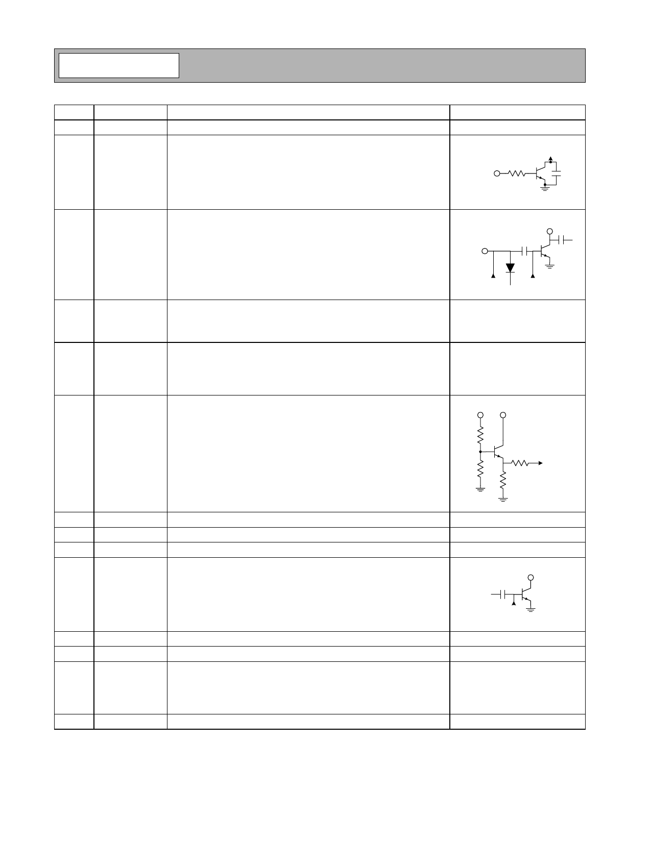
Pin
1
2
3
4
5
6
7
8
9
10
11
12
13
14
Function
GND
AT_EN
RF IN
GND1
VCC1
APC1
Description
Interface Schematic
Internally connected to the ground slug.
See pin 15.
Control input for the PIN diode. The purpose of the PIN diode is to
attenuate the RF input drive level when the VAPC is low. This serves
both to reduce the leakage through the device cause by self biasing
when driving with high level at the RF input, as well as to maintain a
good input match when the bias of the input stage is turned off. When
this pin is “high” the PIN diode control is turned on. See the Theory of
Operation for more details.
RF Input. This is a 50Ω input, but the actual impedance depends on the
interstage matching network connected to pin 5. An external DC block-
ing capacitor is required if this port is connected to a DC path to ground
or a DC voltage.
AT_EN
3k Ω
To PIN
diode
GND1
VCC1
RF IN
PIN
GND 1
From Attn
From Bias
control circuit Stages
Ground connection for the pre-amplifier stage. Keep traces physically
short and connect immediately to the ground plane for best perfor-
mance. It is important for stability that this pin has it’s own vias to the
groundplane, to minimize any common inductance.
Power supply for the pre-amplifier stage and interstage matching. This
pin forms the shunt inductance needed for proper tuning of the inter-
stage match. Please refer to the application schematic for proper con-
figuration, and note that position and value of the components are
important.
Power Control for the driver stage and pre-amplifier. When this pin is
"low," all circuits are shut off. A "low" is typically 0.5V or less at room
temperature. A shunt bypass capacitor is required. During normal oper-
ation this pin is the power control. Control range varies from about 1.0V
for -10dBm to 2.6V for +33dBm RF output power. The maximum power
that can be achieved depends on the actual output matching; see the
application information for more details. The maximum current into this
pin is 5mA when VAPC1=2.6V, and 0mA when VAPC=0V.
See pin 3.
See pin 3.
APC VCC
To RF
Stages
APC2
VCC
GND
RF OUT
Power Control for the output stage. See pin 6 for more details.
GND
GND
See pin 6.
Power supply for the bias circuits.
See pin 6.
Internally connected to the ground slug.
RF Output and power supply for the output stage. Bias voltage for the
final stage is provided through this wide output pin. An external match-
ing network is required to provide the optimum load impedance.
RF OUT
RF OUT
RF OUT
2F0
VCC2
Same as pin 10.
From Bias
Stages GND
PCKG BAS
Same as pin 10.
Same as pin 10.
Same as pin 10.
Connection for the second harmonic trap. This pin is internally con-
nected to the RF OUT pins. The bonding wire together with an external
capacitor form a series resonator that should be tuned to the second
harmonic frequency in order to increase efficiency and reduce spurious
outputs.
Same as pin 15.
Same as pin 10.
2-278
Rev A8 060918
Share Link: 