M27V320-100M1 Просмотр технического описания (PDF) - STMicroelectronics
Номер в каталоге
Компоненты Описание
производитель
M27V320-100M1 Datasheet PDF : 15 Pages
| |||
M27V320
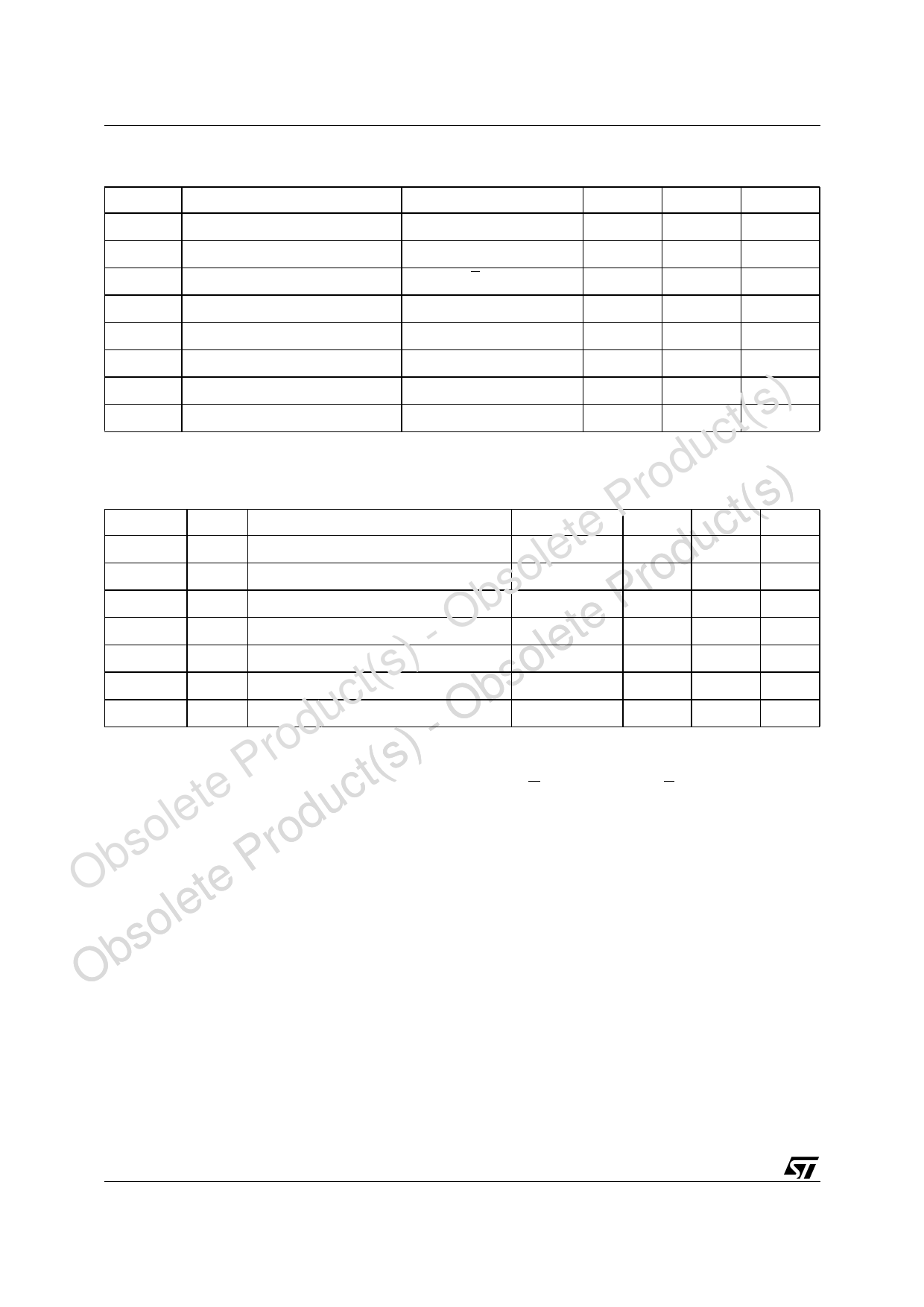
Table 9. Programming Mode DC Characteristics (1)
(TA = 25 °C; VCC = 6.25V ± 0.25V; VPP = 12V ± 0.25V)
Symbol
Parameter
Test Condition
Min
Max
Unit
ILI
Input Leakage Current
VIL ≤ VIN ≤ VIH
±10
µA
ICC
Supply Current
50
mA
IPP
Program Current
E = VIL
50
mA
VIL
Input Low Voltage
–0.3
0.8
V
VIH
Input High Voltage
2.4
VCC + 0.5
V
VOL Output Low Voltage
IOL = 2.1mA
0.4
V
VOH Output High Voltage TTL
IOH = –2.5mA
3.5
V
t(s) VID
A9 Voltage
11.5
12.5
V
c Note: 1. VCC must be applied simultaneously with or before VPP and removed simultaneously or after VPP.
du Table 10. MARGIN MODE AC Characteristics (1)
ro ) (TA = 25 °C; VCC = 6.25V ± 0.25V; VPP = 12V ± 0.25V)
P t(s Symbol
Alt
Parameter
Test Condition Min
lete uc tA9HVPH
tAS9 VA9 High to VPP High
2
so rod tVPHEL
tVPS VPP High to Chip Enable Low
2
b P tA10HEH
tAS10 VA10 High to Chip Enable High (Set)
1
- O te tA10LEH
tAS10 VA10 Low to Chip Enable High (Reset)
1
) le tEXA10X
tAH10 Chip Enable Transition to VA10 Transition
1
t(s so tEXVPX
tVPH Chip Enable Transition to VPP Transition
2
c b tVPXA9X
tAH9 VPP Transition to VA9 Transition
2
du - O Note: 1. VCC must be applied simultaneously with or before VPP and removed simultaneously or after VPP.
Max
Unit
µs
µs
µs
µs
µs
µs
µs
Pro t(s) Programming
te c When delivered, all bits of the M27V320 are in the
le u '1' state. Data is introduced by selectively pro-
d gramming '0's into the desired bit locations. Al-
so ro though only '0's will be programmed, both '1's and
OObbsolete P '0's can be present in the data word. The M27V320
is in the programming mode when VPP input is at
12.5V, GVPP is at VIH and E is pulsed to VIL. The
data to be programmed is applied to 16 bits in par-
allel to the data output pins. The levels required for
the address and data inputs are TTL. VCC is spec-
ified to be 6.25V ± 0.25V.
8/15
Share Link: 