1SMBXXCAT3 Просмотр технического описания (PDF) - ON Semiconductor
Номер в каталоге
Компоненты Описание
производитель
1SMBXXCAT3 Datasheet PDF : 6 Pages
| |||
1SMB10CAT3 Series
MAXIMUM RATINGS
Rating
Symbol
Value
Unit
Peak Power Dissipation (Note 1.)
@ TL = 25°C, Pulse Width = 1 ms
DC Power Dissipation @ TL = 75°C
Measured Zero Lead Length (Note 2.)
Derate Above 75°C
Thermal Resistance from Junction−to−Lead
DC Power Dissipation (Note 3.) @ TA = 25°C
Derate Above 25°C
Thermal Resistance from Junction−to−Ambient
Operating and Storage
Temperature Range
PPK
PD
RqJL
PD
RqJA
TJ, Tstg
600
3.0
40
25
0.55
4.4
226
−65 to +150
W
W
mW/°C
°C/W
W
mW/°C
°C/W
°C
Maximum ratings are those values beyond which device damage can occur. Maximum ratings applied to the device are individual stress limit
values (not normal operating conditions) and are not valid simultaneously. If these limits are exceeded, device functional operation is not
implied, damage may occur and reliability may be affected.
1. 10 X 1000 ms, non−repetitive
2. 1″ square copper pad, FR−4 board
3. FR−4 board, using ON Semiconductor minimum recommended footprint, as
shown in 403A case outline dimensions spec.
*Please see 1SMB5.0AT3 to 1SMB170AT3 for Unidirectional devices.
ELECTRICAL CHARACTERISTICS
(TA = 25°C unless otherwise noted)
Symbol
Parameter
IPP
VC
VRWM
IR
VBR
IT
Maximum Reverse Peak Pulse Current
Clamping Voltage @ IPP
Working Peak Reverse Voltage
Maximum Reverse Leakage Current @ VRWM
Breakdown Voltage @ IT
Test Current
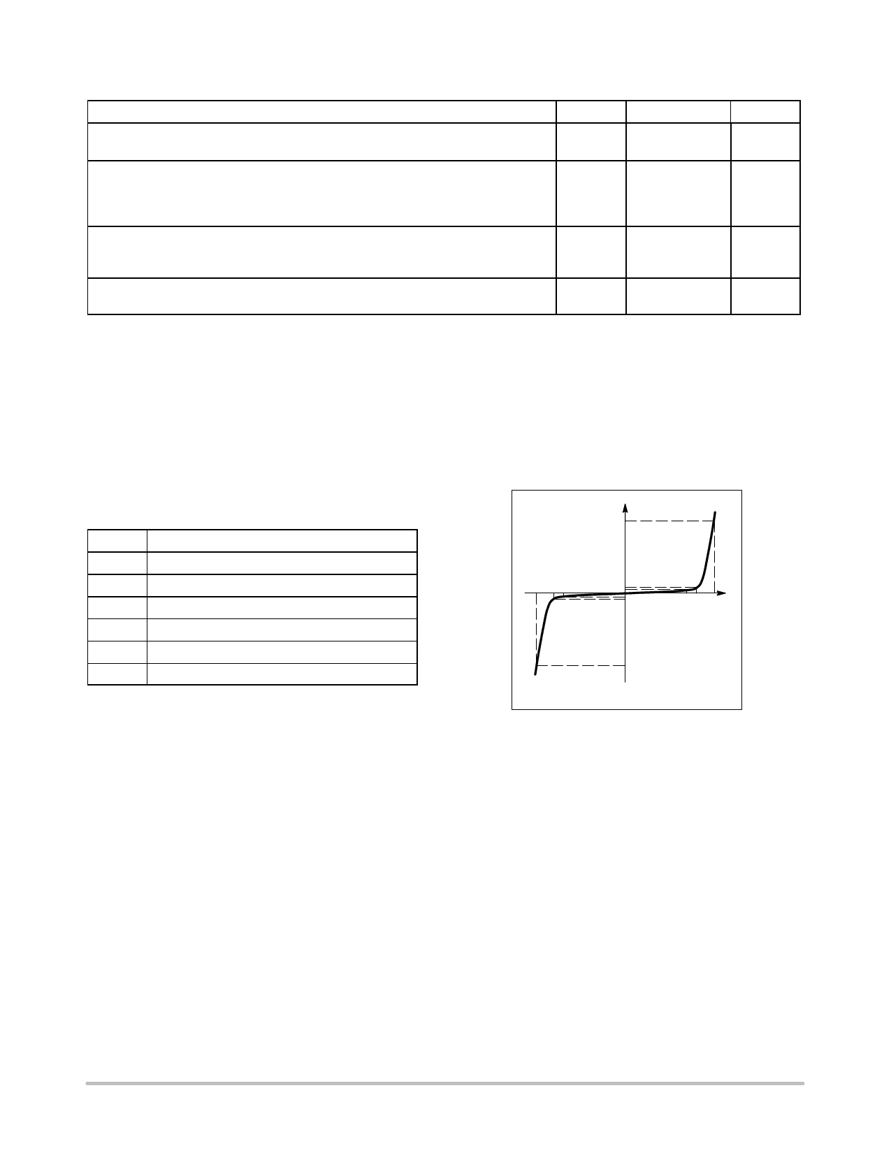
I
IPP
VC VBR VRWM IIRT
IIRT
VRWM VBR VC V
IPP
Bi−Directional TVS
http://onsemi.com
2
Share Link: 