ATF1500AL-25AC Просмотр технического описания (PDF) - Atmel Corporation
Номер в каталоге
Компоненты Описание
производитель
ATF1500AL-25AC Datasheet PDF : 16 Pages
| |||
ATF1500A/AL
The ATF1500A has 32 bi-directional I/O pins and 4 dedi-
cated input pins. Each dedicated input pin can also serve
as a global control signal: register clock, register reset or
output enable. Each of these control signals can be
selected for use individually within each macrocell.
Each of the 32 logic macrocells generates a buried feed-
back, which goes to the global bus. Each input and I/O pin
also feeds into the global bus. Because of this global bus-
sing, each of these signals is always available to all 32
macrocells in the device.
Each macrocell also generates a foldback logic term, which
goes to a regional bus. All signals within a regional bus are
connected to all 16 macrocells within the region.
Cascade logic between macrocells in the ATF1500A allows
fast, efficient generation of complex logic functions. The
ATF1500A contains 4 such logic chains, each capable of
creating sum term logic with a fan in of up to 40 product
terms.
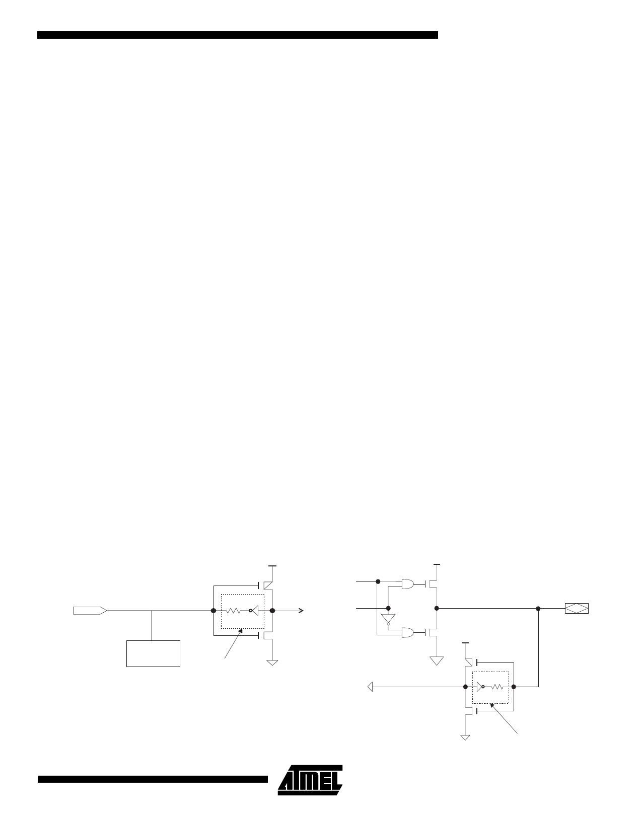
Bus Friendly Pin-Keeper Input and I/O’s
All Input and I/O pins on the ATF1500A have programma-
ble “data keeper” circuits. If activated, when any pin is
driven high or low and then subsequently left floating, it will
stay at that previous high or low level.
This circuitry prevents unused Input and I/O lines from
floating to intermediate voltage levels, which cause unnec-
essary power consumption and system noise. The keeper
circuits eliminate the need for external pull-up resistors and
eliminate their DC power consumption.
Pin-keeper circuits can be disabled. Programming is con-
trolled in the logic design file. Once the pin-keeper circuits
are disabled, normal termination procedures are required
for unused inputs and I/Os.
Speed/Power Management
The ATF1500A has several built-in speed and power man-
agement features. The ATF1500A contains circuitry that
automatically puts the device into a low power stand-by
mode when no logic transitions are occurring. This not only
reduces power consumption during inactive periods, but
also provides a proportional power savings for most appli-
cations running at system speeds below 10 MHz.
All ATF1500As also have an optional pin-controlled power
down mode. In this mode, current drops to below 10 µA.
When the power down option is selected, the PD pin is
used to power down the part. The power down option is
selected in the design source file. When enabled, the
device goes into power down when the PD pin is high. In
the power down mode, all internal logic signals are latched
and held, as are any enabled outputs. All pin transitions are
ignored until the PD is brought low. When the power down
feature is enabled, the PD cannot be used as a logic input
or output. However, the PD pin's macrocell may still be
used to generate buried foldback and cascade logic sig-
nals.
Each output also has individual slew rate control. This may
be used to reduce system noise by slowing down outputs
that do not need to operate at maximum speed. Outputs
default to slow switching, and may be specified as fast
switching in the design file.
Design Software Support
ATF1500A designs are supported by several 3rd party
tools. Automated fitters allow logic synthesis using a variety
of high level description languages and formats.
Input Diagram
I/O Diagram
VCC
VCC
OE
INPUT
DATA
I/O
100K
VCC
ESD
PROTECTION
CIRCUIT
PROGRAMMABLE
OPTION
100K
PROGRAMMABLE
OPTION
3
Share Link: 