GAL22V10C-10LJ Просмотр технического описания (PDF) - Lattice Semiconductor
Номер в каталоге
Компоненты Описание
производитель
GAL22V10C-10LJ Datasheet PDF : 29 Pages
| |||
SpSepceifcicifaictaiotniosnGs AGLA2L22V21V01D0
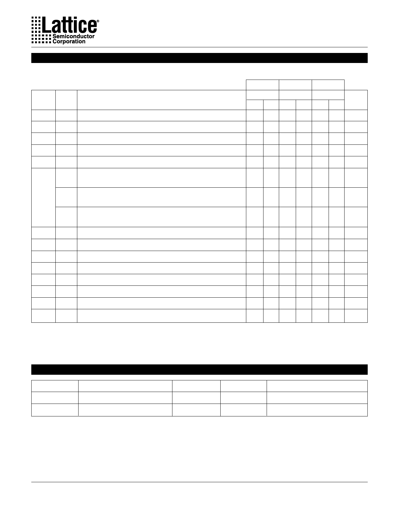
AC Switching Characteristics
Over Recommended Operating Conditions
TEST
PARAM COND.1
DESCRIPTION
tpd
A Input or I/O to Combinatorial Output
tco
A Clock to Output Delay
tcf2
— Clock to Feedback Delay
tsu
— Setup Time, Input or Fdbk before Clk↑
th
— Hold Time, Input or Fdbk after Clk↑
A Maximum Clock Frequency with
External Feedback, 1/(tsu + tco)
fmax3
A Maximum Clock Frequency with
Internal Feedback, 1/(tsu + tcf)
A Maximum Clock Frequency with
No Feedback
twh
— Clock Pulse Duration, High
twl
— Clock Pulse Duration, Low
ten
B Input or I/O to Output Enabled
tdis
C Input or I/O to Output Disabled
tar
A Input or I/O to Asynch. Reset of Reg.
tarw
tarr
tspr
— Asynch. Reset Pulse Duration
— Asynch. Reset to Clk↑ Recovery Time
— Synch. Preset to Clk↑ Recovery Time
COM
COM
COM/IND
-4
-5
-7
UNITS
MIN. MAX. MIN. MAX. MIN. MAX.
1 4 1 5 1 7.5 ns
1 3.5 1 4 1 4.5 ns
— 2.5 — 3 — 3 ns
2.5 — 3 — 4.5 — ns
0 — 0 — 0 — ns
167 — 142.8 — 111 — MHz
200 — 166 — 133 — MHz
250 — 200 — 166 — MHz
2 — 2.5 — 3 — ns
2 — 2.5 — 3 — ns
1 5 1 6 1 7.5 ns
1 5 1 5.5 1 7.5 ns
1 4.5 1 5.5 1 9 ns
4.5 — 4.5 — 7 — ns
3 — 4 — 5 — ns
3 — 4 — 5 — ns
1) Refer to Switching Test Conditions section.
2) Calculated from fmax with internal feedback. Refer to fmax Description section.
3) Refer to fmax Description section. Characterized initially and after any design or process changes that may affect these
parameters.
Capacitance (TA = 25°C, f = 1.0 MHz)
SYMBOL
PARAMETER
CI
Input Capacitance
CI/O
I/O Capacitance
*Characterized but not 100% tested.
MAXIMUM*
8
8
UNITS
pF
pF
TEST CONDITIONS
VCC = 5.0V, VI = 2.0V
VCC = 5.0V, VI/O = 2.0V
7
Share Link: 