VN16218L2 Просмотр технического описания (PDF) - Vaishali Semiconductor
Номер в каталоге
Компоненты Описание
производитель
VN16218L2 Datasheet PDF : 11 Pages
| |||
VN16218
Table 10. DC Electrical Specifications for LVTTL Inputs
TA = 0°C to +70°C, VDDT = 3.15 V to 3.45 V. VDD = 1.7V to 1.9V
Symbol
Parameter
Conditions
VIH
Input High Voltage Level
VIL
Input Low Voltage Level
Table 11. Transmitter Timing Characteristics
TA = 0°C to +70°C, VDDT = 3.15 V to 3.45 V, VDD = 1.7V to 1.9V
Symbol
Parameter
Min.
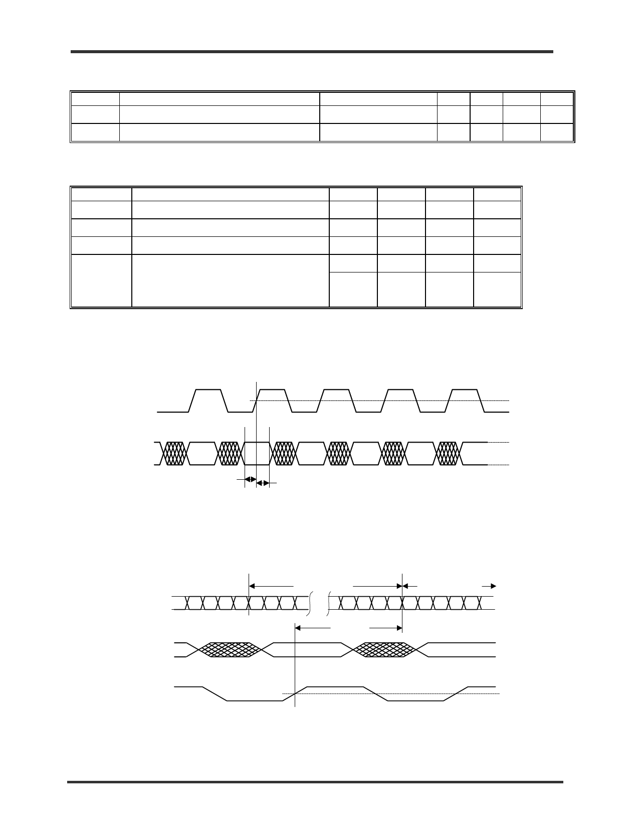
tsetup
Setup Time to Rising Edge of TBC
1.5
Typ.
Advance Information
Min.
2.00
Typ.
Max.
0.80
Unit
V
V
Max.
Unit
nsec
thold
t_txlat[1]
Hold Time to Rising Edge of TBC
Transmitter Latency
1.0
3.5
nsec
nsec
0.8ns+
8.5 bits
Note:
The transmitter latency, as shown in Figure 6, is defined as the time between the latching in of the parallel data word (as triggered by
the rising edge of the transmit byte clock, TBC) and the transmission of the first serial bit of that parallel word (defined by the rising
edge of the first bit transmitted).
TBC
T19:0
1.4 V
DATA
DATA
DATA
tSETUP
tHOLD
DATA
DATA
Figure 5. Transmitter Section Timing
DATA
2.0 V
0.8 V
DATA BYTE A
DATA BYTE B
DOUT± T15 T16 T17 T18 T19 T0 T1 T2
T16 T17 T18 T19 T0 T1 T2 T3 T4 T5
T19:0
t_TXLAT
DATA BYTE B
DATA BYTE C
TBC
1.4 V
Figure 6. Transmitter Latency
2001-11-09
Page 8
MDSN-0003-00
www.vaishali.com
Vaishali Semiconductor 747 Camden Avenue, Suite C Campbell CA 95008 Ph. 408.377.6060 Fax 408.377.6063
Share Link: 