RF2494 Просмотр технического описания (PDF) - RF Micro Devices
Номер в каталоге
Компоненты Описание
производитель
RF2494 Datasheet PDF : 14 Pages
| |||
RF2494
Preliminary
Pin
13
14
15
16
Function
LNA OUT
VCC4
Description
RF signal output for external 50Ω filtering.The use of a filter here is
optional but does provide for lower noise floor and better out-of-band
rejection.
Supply voltage for the LNA. This pin should be bypassed with a 10 pF
capacitor to ground as close to the pin as possible. The shunt induc-
tance from this pin to ground via the supply decoupling must be tuned
to match the LNA output to 50Ω at the desired operating frequency.
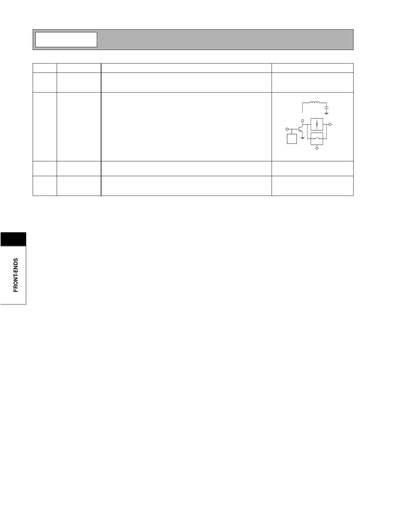
Interface Schematic
See pin 14.
Microstrip
VCC4 -16 dB
P2
LNA IN
BIAS
EXTERNAL
DECOUPLING
P15
LNA OUT
GS
LNA IN
LNA gain control. When GAIN SEL is >VCC- 300mV, LNA gain is at 10
dB. When GAIN SEL is <300mV, the LNA gain is -6dB.
This pin is NOT internally DC blocked. An external blocking capacitor
must be provided if the pin is connected to a device with DC present. If
a blocking capacitor is required, a value of 2pF is recommended.
See pin 14.
See pin 14.
P1
GAIN SEL
8
8-56
Rev A0 010730
Share Link: 