TS482(2003) Просмотр технического описания (PDF) - STMicroelectronics
Номер в каталоге
Компоненты Описание
производитель
TS482 Datasheet PDF : 24 Pages
| |||
TS482
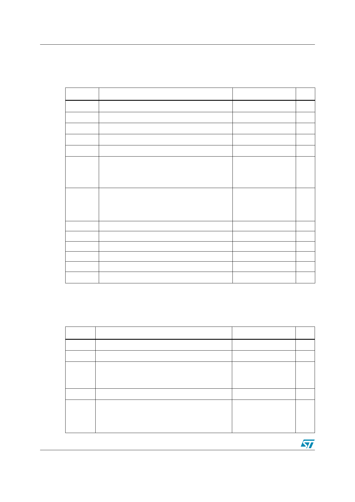
ABSOLUTE MAXIMUM RATINGS
Symbol
Parameter
Value
Unit
VCC Supply voltage 1)
6
V
Vi Input Voltage
-0.3 to VCC +0.3
V
Toper Operating Free Air Temperature Range
-40 to + 85
°C
Tstg Storage Temperature
-65 to +150
°C
Tj Maximum Junction Temperature
150
°C
Rthja
Thermal Resistance Junction to Ambient
SO8
MiniSO8
DFN8
175
215
°C/W
70
Power Dissipation 2)
Pd
SO8
MiniSO8
DFN8
0.71
0.58
W
1.79
ESD Human Body Model (pin to pin)
2
kV
ESD Machine Model - 220pF - 240pF (pin to pin)
200
V
Latch-up Latch-up Immunity (All pins)
200
mA
Lead Temperature (soldering, 10sec)
250
°C
Output Short-Circuit Duration
see note 3)
1. All voltages values are measured with respect to the ground pin.
2. Pd has been calculated with Tamb = 25°C, Tjunction = 150°C.
3. Attention must be paid to continuous power dissipation. Exposure of the IC to a short circuit on one or two amplifiers simultaneously can cause exces-
sive heating and the destruction of the device.
OPERATING CONDITIONS
Symbol
Parameter
VCC Supply Voltage
RL Load Resistor
Load Capacitor
CL
RL = 16 to 100Ω
RL > 100Ω
VICM Common Mode Input Voltage Range
RTHJA
Thermal Resistance Junction to Ambient
SO8
MiniSO8
DFN81)
1. When mounted on a 4-layer PCB.
Value
2 to 5.5
>= 16
400
100
GND to VCC
150
190
41
Unit
V
Ω
pF
V
°C/W
Components
Functional Description
Rin
Cin
Rfeed
Cs
Cb
Cout
Rpol
Av
Inverting input resistor which sets the closed loop gain in conjunction with Rfeed. This resistor also
forms a high pass filter with Cin (fc = 1 / (2 x Pi x Rin x Cin))
Input coupling capacitor which blocks the DC voltage at the amplifier input terminal
Feed back resistor which sets the closed loop gain in conjunction with Rin
Supply Bypass capacitor which provides power supply filtering
Bypass capacitor which provides half supply filtering
Output coupling capacitor which blocks the DC voltage at the load input terminal
This capacitor also forms a high pass filter with RL (fc = 1 / (2 x Pi x RL x Cout))
These 2 resistors form a voltage divider which provide a DC biasing voltage (Vcc/2) for the 2 amplifiers.
Closed loop gain = -Rfeed / Rin
2/24
Share Link: 