IRFL4310 Просмотр технического описания (PDF) - International Rectifier
Номер в каталоге
Компоненты Описание
производитель
IRFL4310 Datasheet PDF : 9 Pages
| |||
IRFL4310
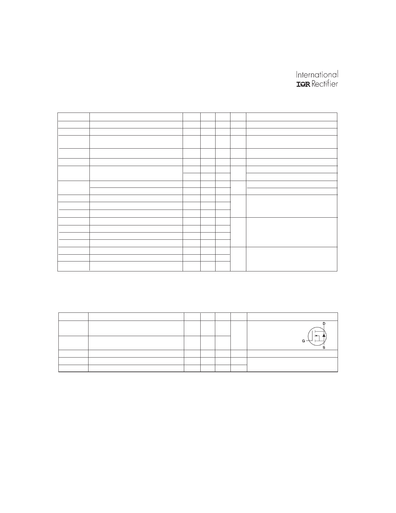
Electrical Characteristics @ TJ = 25°C (unless otherwise specified)
Parameter
V(BR)DSS Drain-to-Source Breakdown Voltage
DV(BR)DSS/DTJ Breakdown Voltage Temp. Coefficient
RDS(on)
Static Drain-to-Source On-Resistance
Min.
100
Typ.
0.12
Max.
0.20
Units
V
V/°C
W
Conditions
VGS = 0V, ID = 250µA
Reference to 25°C, ID = 1mA
VGS = 10V, ID = 1.6A
VGS(th)
gfs
IDSS
IGSS
Qg
Qgs
Qgd
td(on)
tr
td(off)
tf
Ciss
Coss
Crss
Gate Threshold Voltage
Forward Transconductance
Drain-to-Source Leakage Current
Gate-to-Source Forward Leakage
Gate-to-Source Reverse Leakage
Total Gate Charge
Gate-to-Source Charge
Gate-to-Drain ("Miller") Charge
Turn-On Delay Time
Rise Time
Turn-Off Delay Time
Fall Time
Input Capacitance
Output Capacitance
Reverse Transfer Capacitance
2.0
1.5
4.0
25
250
100
-100
17 25
2.1 3.1
7.8 12
7.8
18
34
20
330
92
54
V VDS = VGS, ID = 250µA
S VDS = 50V, ID = 0.80 A
µA VDS = 100V, VGS = 0V
VDS = 80V, VGS = 0V, TJ = 125°C
nA VGS = 20V
VGS = -20V
ID = 1.6A
nC VDS = 80V
VGS = 10V, See Fig. 6 and 13
VDD = 50V
ns ID = 1.6A
RG = 6.2 W
RD = 31 W, See Fig. 10
VGS = 0V
pF VDS = 25V
= 1.0MHz, See Fig. 5
Source-Drain Ratings and Characteristics
Parameter
IS
Continuous Source Current
(Body Diode)
ISM
Pulsed Source Current
(Body Diode)
VSD
Diode Forward Voltage
trr
Reverse Recovery Time
Qrr
Reverse RecoveryCharge
Min.
Typ.
72
210
Max. Units
0.91
A
13
1.3 V
110 ns
320 nC
Conditions
MOSFET symbol
showing the
integral reverse
p-n junction diode.
TJ = 25°C, IS = 1.6A, VGS = 0V
TJ = 25°C, IF = 1.6A
di/dt = 100A/µs
Notes:
Repetitive rating; pulse width limited by
max. junction temperature. ( See fig. 11 )
VDD = 25V, starting TJ = 25°C, L = 9.2 mH
RG = 25W, IAS = 3.2A. (See Figure 12)
2
ISD £ 1.6A, di/dt £ 340A/µs, VDD £ V(BR)DSS,
TJ £ 150°C
Pulse width £ 300µs; duty cycle £ 2%.
www.irf.com
Share Link: 