UPC8204TK-E2-A(2005) Просмотр технического описания (PDF) - California Eastern Laboratories.
Номер в каталоге
Компоненты Описание
производитель
UPC8204TK-E2-A Datasheet PDF : 4 Pages
| |||
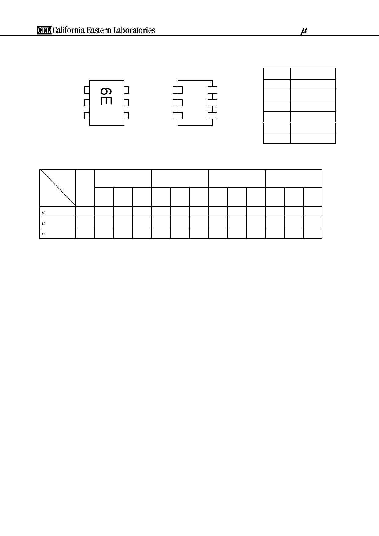
UPC8204TK
ABSOLUTE MAXIMUM RATINGS1 (TA = 25°C)
SYMBOLS
PARAMETERS
UNITS RATINGS
VCC
Supply Voltage TA = 25°C
V
3.6
ICC
Total Circuit Current
TA = 25°C
mW
30
VAGC
Gain Control Voltage
TA = 25°C
V
3.6
PD
Power Dissipation
TA = 85°C (note)
mW
203
TA
Operating Ambient
Temperature
°C
-40 to +85
TSTG
Storage Temperature
°C -55 to +150
PIN
Input Power
dBm
+5
Notes:
1. Mounted on a 50 x 50 x 1.6 mm epoxy glass PWB (TA = +85°C).
RECOMMENDED
OPERATING CONDITIONS
SYMBOLS PARAMETERS
VCC
Supply Voltage
TA
Operating Ambient
Temperature
fin
Operating Frequency
Range
VAGC
Gain Control
Voltage
UNITS MIN TYP MAX
V 2.7 3.0 3.3
°C -40 +25 +85
GHz 0.8 – 2.5
V
0 – 3.3
SERIES PRODUCTS
Parameter
Part No.
UPC8119T
UPC8120T
UPC8204TK
ICC
(mA)
11.0
11.0
11.5
0.95 GHz output port
matching frequency
GPMAX GCR
NF
(dB) (dB)
12.5 50
(dB)
8.5
13.0 50
9.0
–
–
–
1.44 GHz output port
matching frequency
GPMAX GCR
NF
(dB)
13.0
(dB)
45
(dB)
7.5
13.5
45
7.5
–
–
–
1.9 GHz output port
matching frequency
GPMAX GCR
NF
(dB) (dB)
(12.5) (22)
(dB)
(7.2)
(13.0) (22)
(7.3)
14.0
40
7.5
Note:
1. Typical performance. Please refer to Electrical Charateristics in detail.
( ): Reference
2.4 GHz output port
matching frequency
GPMAX GCR NF
–
–
–
–
–
–
14.0
35
7.5
PIN FUNCTIONS
Pin No. Symbol Applied Voltage Pin Voltage
Description
1
INPUT
—
2
GND
0
3
1.2
RF input pin This pin should be
coupled with capacitor (eg 1000 pF)
for DC cut. Input return loss can be
improved with external impedance
matching circuit.
—
Ground pin. This pin should be
GROUND
connected to system ground with
CIRCUIT
minimum inductance. Ground
pattern on the board should be
formed as wide as possible. Ground
pins must be connected together with
wide ground pattern to decrease
impedance difference.
4
OUTPUT Voltage as same
—
as VCC through
external inductor
RF output pin. This pin is designed
as open collector of high impedance.
This pin must be externally equipped
with matching circuits.
5
VCC
2.7~3.3
—
Supply voltage pin. this pin must be
equipped with bypass capacitor
(eg 1000 pF) to minimize its RF
impedance.
6
VAGC
0~3.3
—
Gain control pin.
6
Equivalent Circuit
5
4
1
BIAS
CIRCUIT
2
3
GND
5
CONTROL CIRCUIT
2
Share Link: 