UPC2791TB Просмотр технического описания (PDF) - California Eastern Laboratories.
Номер в каталоге
Компоненты Описание
производитель
UPC2791TB Datasheet PDF : 4 Pages
| |||
ABSOLUTE MAXIMUM RATINGS1 (TA = 25°C)
SYMBOLS
PARAMETERS
UNITS RATINGS
VCC Supply Voltage
V
6
PIN
Input Power
dBm
+10
PT
Total Power Dissipation2
mW
200
TOP Operating Temperature
°C
-40 to +85
TSTG Storage Temperature
°C -55 to +150
Notes:
1. Operation in excess of any one of these parameters may result
in permanent damage.
2. Mounted on double sided copper clad 50 x 50 x 1.6 mm epoxy
glass PWB (TA = +85°C).
UPC2791TB, UPC2792TB
RECOMMENDED
OPERATING CONDITIONS
SYMBOL
PARAMETER
UNITS MIN TYP MAX
VCC Supply Voltage
V 4.5 5.0 5.5
TOP Operating Temperature ˚C -40 +25 +85
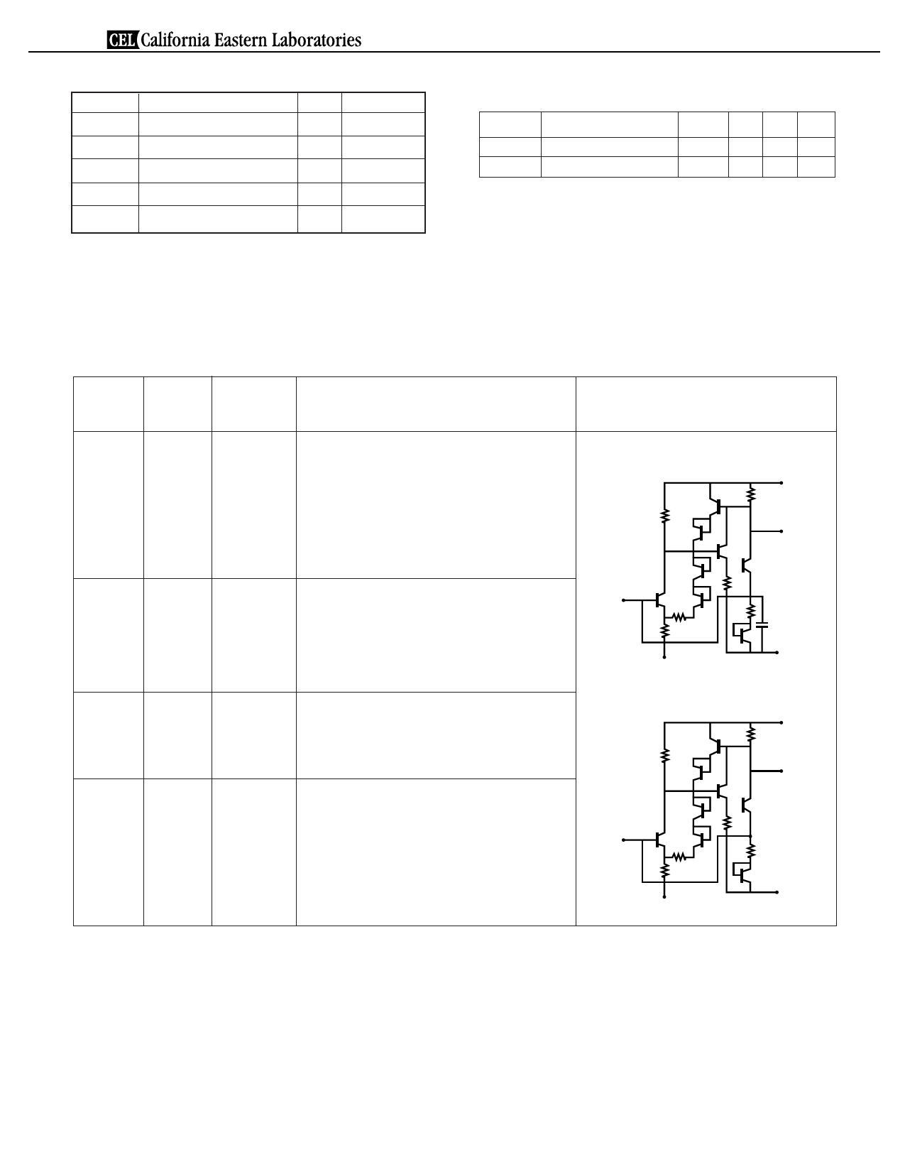
PIN DESCRIPTION
Pin
Pin
No.
Name
Applied
Voltage
(V)
1
GND
0
2
5
3
Output
—
4
VCC
4.5 to 5.5
6
Input
—
Description
Ground pin. This pin should be connected
to system ground with minimum inductance.
Ground pattern on the board should be
formed as wide as possible. All the ground
pins must be connected together with wide
ground pattern to minimize impedance
difference.
Signal output pin. An internal matching
circuit, configured with resistors, enables
50 Ω connection over a wide bandwidth.
This pin must be coupled to the output
load with a blocking capacitor.
Power supply pin. This pin should be
externally equipped with a bypass capacitor
to minimize ground impedance.
Signal input pin. An internal matching
circuit, configured with resistors, enables
50 Ω connection over a wide bandwidth.
A multi-feedback circuit is designed to
cancel the deviations of hFE and resistance.
This pin must be coupled to the signal source
with a blocking capacitor.
Internal Equivalent Circuit
UPC2791TB
VCC
OUT
IN
GND1
UPC2792TB
GND2
VCC
OUT
IN
GND1
GND2
Share Link: 