UPC2747TB Просмотр технического описания (PDF) - California Eastern Laboratories.
Номер в каталоге
Компоненты Описание
производитель
UPC2747TB Datasheet PDF : 9 Pages
| |||
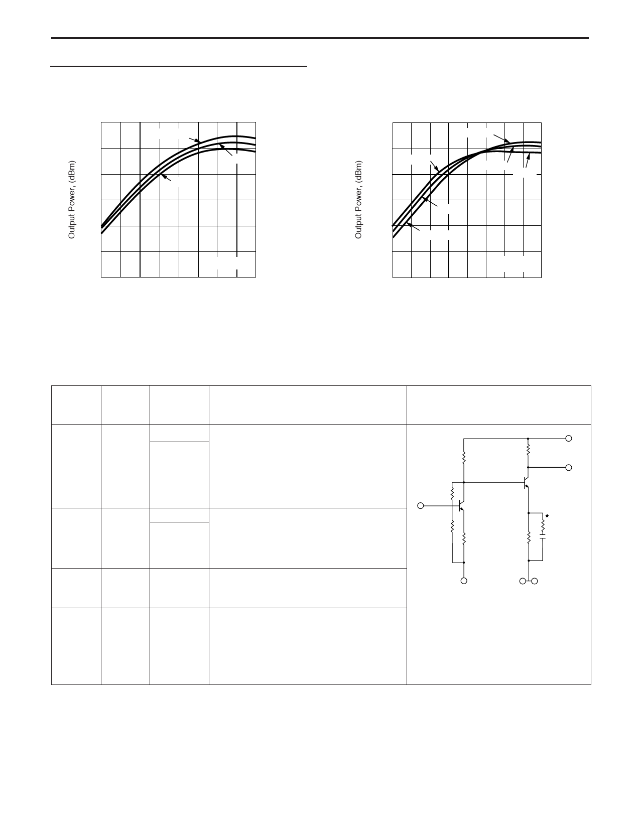
TYPICAL PERFORMANCE CURVES (TA = 25°C)
UPC2748TB
OUTPUT POWER vs. INPUT POWER
AND VOLTAGE
0
VCC = 3.3 V
3.0 V
-10
2.7 V
-20
-30
-40
f = 900 MHZ
-30
-20
-10
0
Input Power, PIN (dBm)
UPC2747TB, UPC2748TB
UPC2748TB
OUTPUT POWER vs. INPUT POWER
AND TEMPERATURE
0
TA = +85˚ C
-40 ˚ C
-10
+25˚ C
-40 ˚ C
+25˚ C
-20
TA = +85˚ C
-30
-40
VCC = 3.0 V
f = 900 MHZ
-30
-20
-10
0
Input Power, PIN (dBm)
PIN DESCRIPTION
Pin
Pin
Applied
No.
Name
Voltage
(V)
1
Input
0.81
0.82
4
Output
2.791
2.722
6
VCC
2.7 to 3.3
2
GND
0
3
5
Notes:
1. UPC2747TB.
2. UPC2748TB.
Description
Internal Equivalent Circuit
Signal input pin. An internal matching
circuit, configured with resistors, enables
50 Ω connection over a wide bandwidth.
A multi-feedback circuit is designed to
cancel the deviations of hFE and resistance.
This pin must be coupled to the signal source
with a blocking capacitor.
Signal output pin. An internal matching
circuit, configured with resistors, enables
50 Ω connection over a wide bandwidth.
This pin must be coupled to the output
load with a blocking capacitor.
Power supply pin. This pin should be
externally equipped with a bypass capacitor
to minimize ground impedance.
Ground pin. This pin should be connected
to system ground with minimum inductance.
Ground pattern on the board should be
formed as wide as possible. All the ground
pins must be connected together with wide
ground pattern to minimize impedance
difference.
1
IN
VCC
6
OUT
4
3
GND
2
5
GND
The above diagram is for the UPC2747TB.
The resistor marked with a star does not
exist in the UPC 2748TB.
Share Link: 