UESDXXDT5G Просмотр технического описания (PDF) - ON Semiconductor
Номер в каталоге
Компоненты Описание
производитель
UESDXXDT5G Datasheet PDF : 4 Pages
| |||
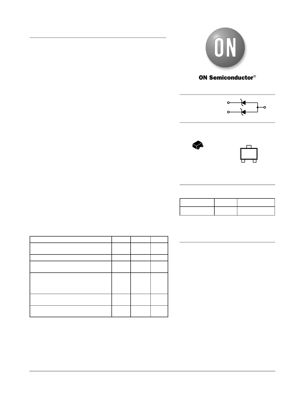
mESD3.3DT5G SERIES
ESD Protection Diodes
In Ultra Small SOT−723 Package
The mESD Series is designed to protect voltage sensitive components
from ESD. Excellent clamping capability, low leakage, and fast response
time, make these parts ideal for ESD protection on designs where board
space is at a premium. Because of its small size, it is suited for use in
cellular phones, portable devices, digital cameras, power supplies and
many other portable applications.
Specification Features:
• Small Body Outline Dimensions:
0.047″ x 0.032″ (1.20 mm x 0.80 mm)
• Low Body Height: 0.020″ (0.5 mm)
• Stand−off Voltage: 3.3 V − 6.0 V
• Low Leakage
• Response Time is Typically < 1 ns
• ESD Rating of Class 3 (> 16 kV) per Human Body Model
• IEC61000−4−2 Level 4 ESD Protection
• IEC61000−4−4 Level 4 EFT Protection
• AEC−Q101 Qualified and PPAP Capable
• These are Pb−Free Devices
Mechanical Characteristics:
CASE: Void-free, transfer-molded, thermosetting plastic
Epoxy Meets UL 94 V−0
LEAD FINISH: 100% Matte Sn (Tin)
MOUNTING POSITION: Any
QUALIFIED MAX REFLOW TEMPERATURE: 260°C
Device Meets MSL 1 Requirements
MAXIMUM RATINGS
Rating
Symbol Value Unit
IEC 61000−4−2 (ESD)
Air
Contact
±30
kV
±30
IEC 61000−4−4 (EFT)
40
A
ESD Voltage
Per Human Body Model
Per Machine Model
16
kV
400
V
Total Power Dissipation on FR−5 Board
(Note 1) @ TA = 25°C
Derate above 25°C
Thermal Resistance Junction−to−Ambient
Junction and Storage Temperature Range
⎪
PD
RqJA
TJ, Tstg
240
1.9
525
−55 to
+150
mW
mW/°C
°C/W
°C
Lead Solder Temperature − Maximum
(10 Second Duration)
TL
260
°C
Stresses exceeding Maximum Ratings may damage the device. Maximum
Ratings are stress ratings only. Functional operation above the Recommended
Operating Conditions is not implied. Extended exposure to stresses above the
Recommended Operating Conditions may affect device reliability.
1. FR−5 = 1.0 x 0.75 x 0.62 in.
http://onsemi.com
PIN 1. CATHODE 1
2. CATHODE
3
3. ANODE
2
3
2
1
SOT−723
CASE 631AA
STYLE 4
MARKING
DIAGRAM
xx M
xx = Device Code
M = Date Code
ORDERING INFORMATION
Device
Package
Shipping†
UESDxxDT5G SOT−723 8000/Tape & Reel
†For information on tape and reel specifications,
including part orientation and tape sizes, please
refer to our Tape and Reel Packaging Specifications
Brochure, BRD8011/D.
DEVICE MARKING INFORMATION
See specific marking information in the device marking
column of the table on page 2 of this data sheet.
© Semiconductor Components Industries, LLC, 2013
1
January, 2013 − Rev. 4
Publication Order Number:
UESD3.3DT5G/D
Share Link: 