CGY2014TT Просмотр технического описания (PDF) - Philips Electronics
Номер в каталоге
Компоненты Описание
производитель
CGY2014TT Datasheet PDF : 16 Pages
| |||
Philips Semiconductors
GSM/DCS/PCS power amplifier
Preliminary specification
CGY2014TT
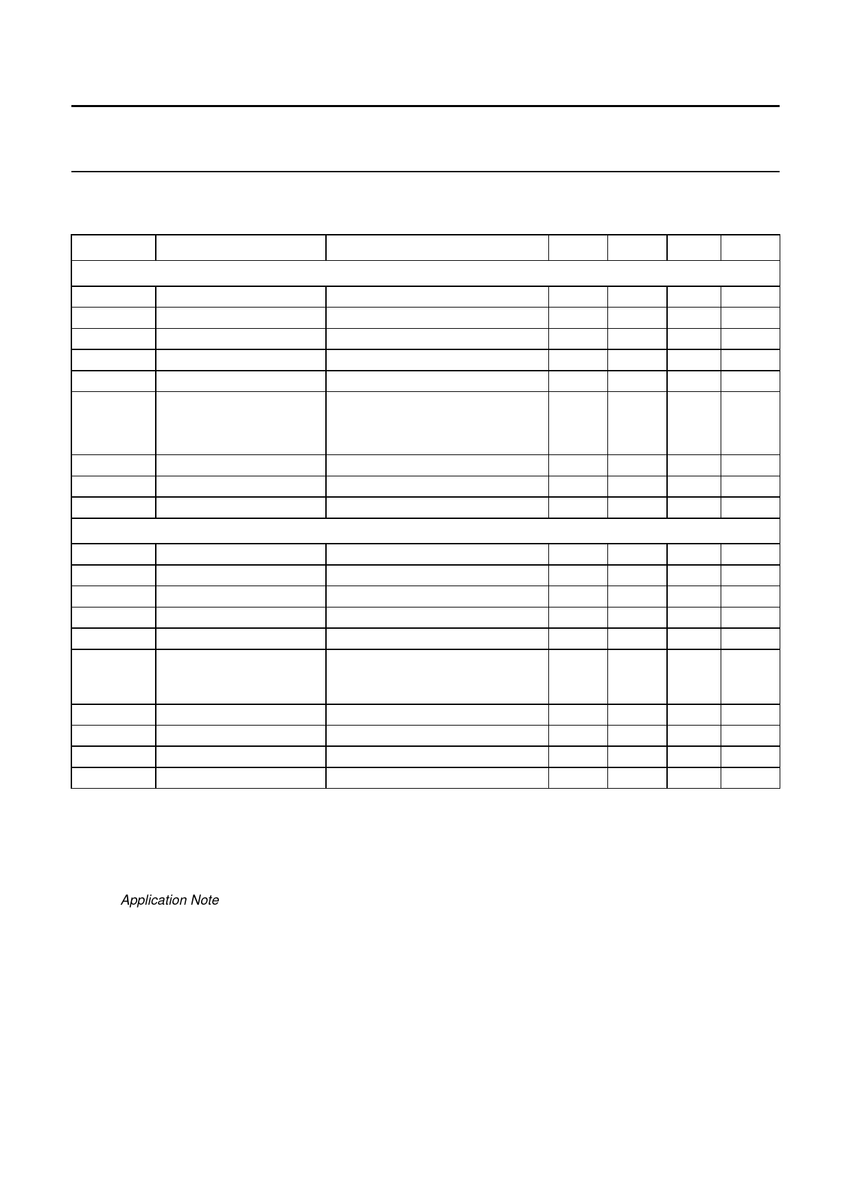
AC CHARACTERISTICS
VDD = 3.5 V; Tamb = 25 °C; measured on the Philips demoboard (see Fig.8).
SYMBOL
PARAMETER
CONDITIONS
MIN. TYP. MAX. UNIT
Low band: GSM power amplifier
Pi(LB)
fRF(LB)
Po(LB)(max)
ηLB
Po(LB)(min)
NRX(LB)
H2LB
H3LB
StabLB
input power
RF frequency range
maximum output power
efficiency
minimum output power
output noise in RX band
2nd harmonic level
3rd harmonic level
stability
see Figs 3 and 4
see Fig.3
VDD = 0 V; Pi(LB) = 0 dBm
Pi(LB) = 0 dBm
fRF = 925 to 935 MHz
fRF = 935 to 960 MHz
Pi(LB) = 0 dBm
Pi(LB) = 0 dBm
Pi(LB) = 0 dBm; note 1
High band: DCS/PCS power amplifier; note 2
−2
0
880
−
34.5 35
50
55
−
−35
−
−
−
−
−
−
−
−
−
−
+2
dBm
915 MHz
−
dBm
−
%
−
dBm
−117
−129
−35
−35
−60
dBm/Hz
dBm/Hz
dBc
dBc
dBc
Pi(HB)
fRF(HB)
Po(HB)(max)
ηHB
Po(HB)(min)
αHB
NRX(HB)
H2HB
H3HB
StabHB
input power
RF frequency range
maximum output power
efficiency
minimum output power
high band isolation when
low band is operating
output noise in RX band
2nd harmonic level
3rd harmonic level
stability
for DCS operation
see Figs 5 and 6
see Fig.5
VDD = 0 V; Pi(HB) = 3 dBm
VDD(LB) = 3.5 V; Pi(LB) = 0 dBm;
VDD(HB) = 0 V; Pi(HB) = 3 dBm;
note 3
Pi(HB) = 3 dBm
Pi(HB) = 3 dBm
Pi(HB) = 3 dBm
Pi(HB) = 3 dBm; note 1
2
3
1710 −
32
32.5
38
40
−
−32
−
0
5
1 785
−
−
−
−
dBm
MHz
dBm
%
dBm
dBm
−
−
−121 dBm/Hz
−
−
−35 dBc
−
−
−35 dBc
−
−
−60 dBc
Notes
1. The device is adjusted to provide nominal load power into a 50 Ω load. The device is switched off and a 6 : 1 load
replaces the 50 Ω load. The device is switched on and the phase of the 6 : 1 load is varied 360 electrical degrees
during a 60 seconds test period.
2. The power amplifier can be matched to PCS and or DCS/PCS operation through optimization of the matching circuit;
see Application Note (tbf).
3. Isolation can be improved to −20 dBm (typical value) with a pin diode switched in the DCS output matching.
2000 Apr 11
6
Share Link: 