CGY2013G/C1 Просмотр технического описания (PDF) - Philips Electronics
Номер в каталоге
Компоненты Описание
производитель
CGY2013G/C1 Datasheet PDF : 12 Pages
| |||
Philips Semiconductors
GSM 4 W power amplifier
Preliminary specification
CGY2013G
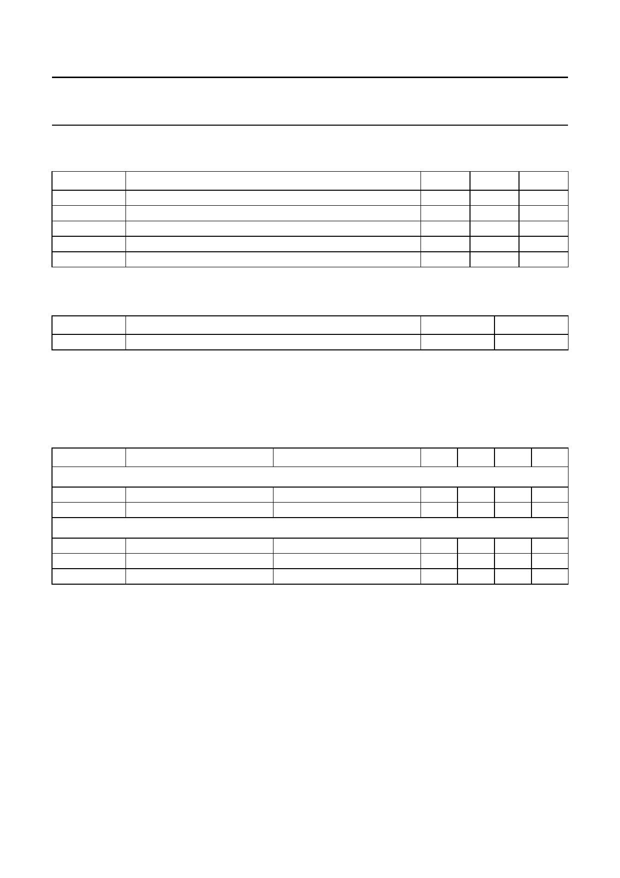
LIMITING VALUES
In accordance with the Absolute Maximum Rating System (IEC 134); general operating conditions applied.
SYMBOL
VDD
VGG
Tj(max)
Tstg
Ptot
PARAMETER
positive supply voltage
negative supply voltage
maximum operating junction temperature
IC storage temperature
total power dissipation
MIN.
−
−
−
−
−
MAX.
7
−10
150
150
1.5
UNIT
V
V
°C
°C
W
THERMAL CHARACTERISTICS
General operating conditions applied.
SYMBOL
Rth j-c
PARAMETER
thermal resistance from junction to case; note 1
Note
1. This thermal resistance is measured under GSM pulse conditions.
VALUE
25
UNIT
K/W
DC CHARACTERISTICS
VDD = 3.6 V; Tamb = 25 °C; general operating conditions applied; peak current values during burst; unless otherwise
specified.
SYMBOL
PARAMETER
CONDITIONS
MIN. TYP. MAX. UNIT
Pins RFO/VDD4, VDD3, VDD2, VDD1 and DETO/VDD5
VDD
positive supply voltage
IDD
positive peak supply current
Pins VGG1 and VGG2
VGG1
VGG2
IGG1 + IGG2
negative supply voltage
negative supply voltage
negative peak supply current
note 1
note 1
0
3.6 5.5 V
−
2.4 3.0 A
−
−1.8 −
V
−
−1.8 −
V
−
2.5 5
mA
Note
1. The negative bias VGG1 and VGG2 must be applied 10 µs before the power amplifier is switched on, and must remain
applied until the power amplifier has been switched off.
1998 Jan 23
5
Share Link: 