CGY2013G Просмотр технического описания (PDF) - Philips Electronics
Номер в каталоге
Компоненты Описание
производитель
CGY2013G Datasheet PDF : 12 Pages
| |||
Philips Semiconductors
GSM 4 W power amplifier
handbook, full pagewidth
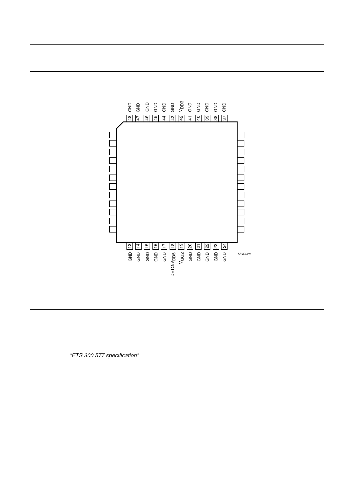
GND 1
GND 2
GND 3
GND 4
RFO/VDD4 5
RFO/VDD4 6
RFO/VDD4 7
RFO/VDD4 8
GND 9
GND 10
GND 11
GND 12
CGY2013G
Preliminary specification
CGY2013G
36 GND
35 GND
34 GND
33 VDD2
32 GND
31 VGG1
30 GND
29 VDD1
28 GND
27 RFI
26 GND
25 GND
MGD628
Fig.2 Pin configuration.
FUNCTIONAL DESCRIPTION
Operating conditions
The CGY2013G is designed to meet the European
Telecommunications Standards Institute (ETSI) GSM
documents, the “ETS 300 577 specification”, which are
defined as follows:
• ton = 542.8 µs
• T = 4.3 ms
• Duty cycle = 1/8.
The device is specifically designed for pulse operation
allowing the use of a LQFP48 plastic package.
Power amplifier
The power amplifier consists of four cascaded gain stages
with an open-drain configuration. Each drain has to be
loaded externally by an adequate reactive circuit which
also has to be a DC path to the supply.
The amplifier bias is set using a negative voltage applied
at pins VGG1 and VGG2. This negative voltage must be
present before the supply voltage is applied to the drains
to avoid current overstress for the amplifier.
1998 Jan 23
4
Share Link: 