NE555 Просмотр технического описания (PDF) - STMicroelectronics
Номер в каталоге
Компоненты Описание
производитель
NE555 Datasheet PDF : 20 Pages
| |||
NE555 - SA555 - SE555
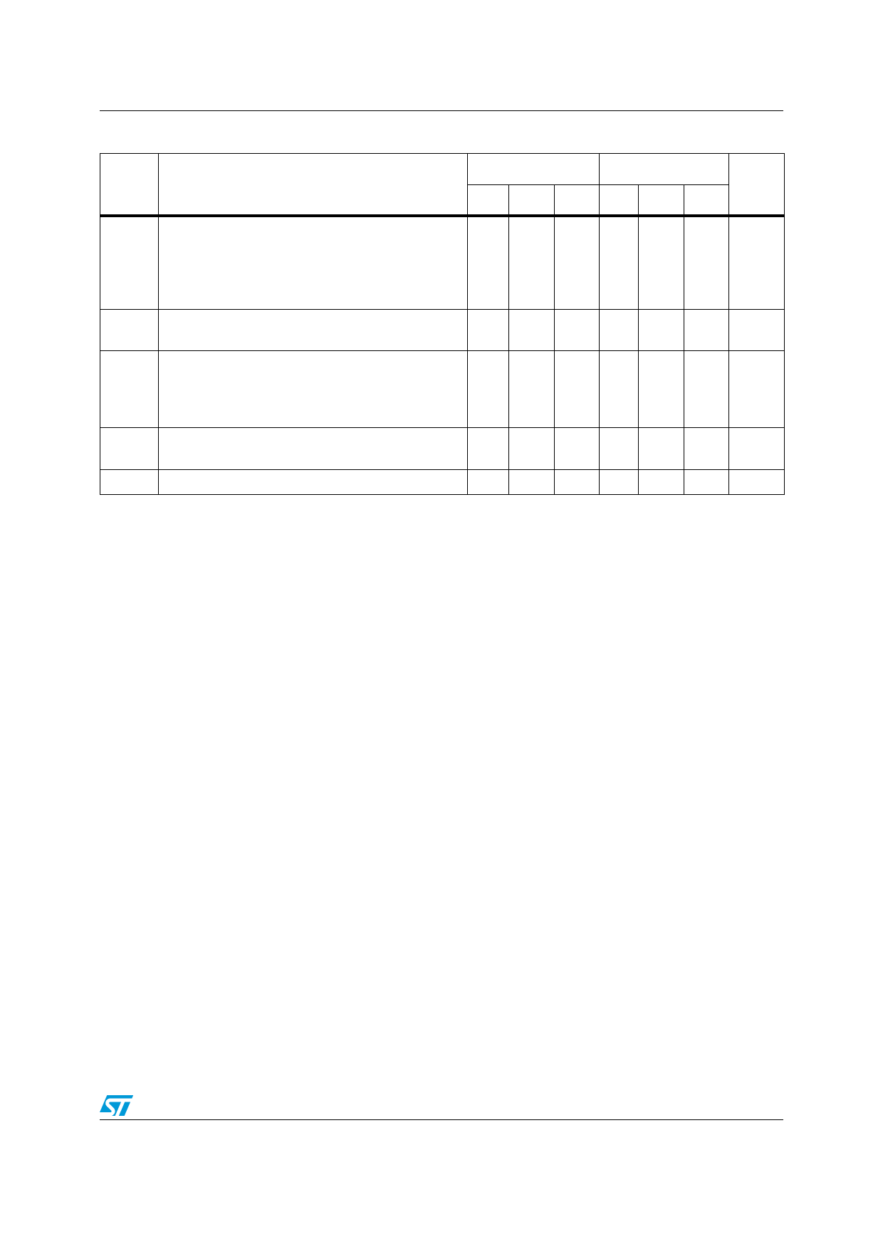
Electrical characteristics
Table 3.
Symbol
Tamb = +25° C, VCC = +5 V to +15 V (unless otherwise specified) (continued)
Parameter
SE555
NE555 - SA555
Unit
Min. Typ. Max. Min. Typ. Max.
High level output voltage
VOH
VCC = +15 VIO(sink) = 200 mA
IO(sink) = 100 mA
VCC = +5 V IO(sink) = 100 mA
12.5
13 13.3
3 3.3
12.7
5
2.75
12.5
13.3
3.3
V
Idis(off)
Discharge pin leakage current
(output high) Vdis = 10 V
Vdis(sat)
Discharge pin saturation voltage
(output low) (4)
VCC = +15V, Idis = 15 mA
VCC = +5V, Idis = 4.5 mA
tr Output rise time
tf Output fall time
toff Turn off time (5) (Vreset = VCC)
20 100
180 480
80 200
100 200
100 200
0.5
20 100 nA
mV
180 480
80 200
100 300
100 300
ns
0.5
µs
1. Tested at VCC = +5 V and VCC = +15 V.
2. This will determine the maximum value of RA + RB for 15 V operation. The maximum total (RA + RB) is 20 MΩ for +15 V
operation and 3.5 MΩ for +5 V operation.
3. Specified with trigger input high.
4. No protection against excessive pin 7 current is necessary, providing the package dissipation rating is not exceeded.
5. Time measured from a positive pulse (from 0 V to 0.8 x VCC) on the threshold pin to the transition from high to low on the
output pin. Trigger is tied to threshold.
Doc ID 2182 Rev 6
5/20
Share Link: 