S-81230SG Просмотр технического описания (PDF) - Seiko Instruments Inc
Номер в каталоге
Компоненты Описание
производитель
S-81230SG Datasheet PDF : 33 Pages
| |||
HIGH PRECISION VOLTAGE REGULATOR
S-812XXSG Series
4. S-81218SG-QR-X (1.8-V output type)
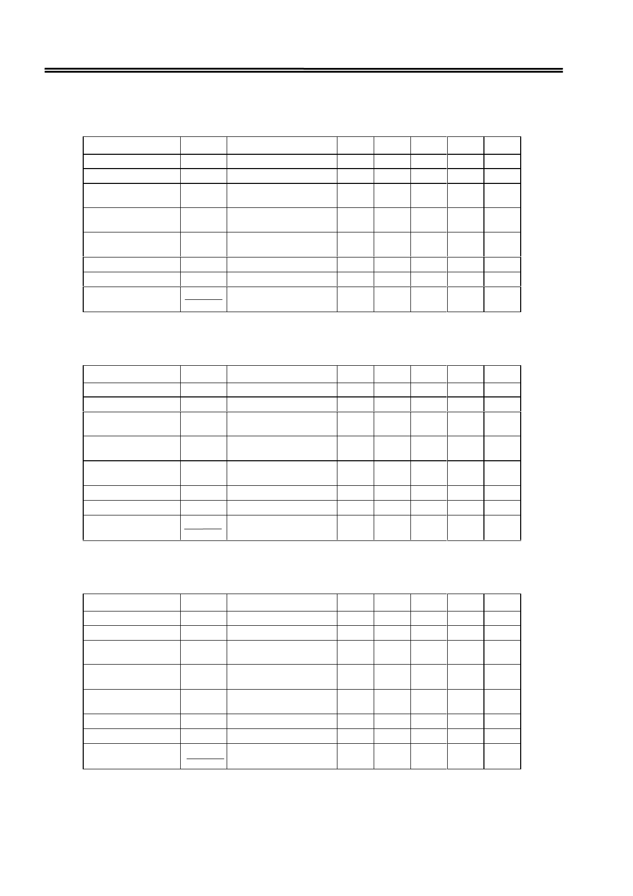
Table 6
Parameter
Output voltage
I/O voltage difference
Line regulation 1
Line regulation 2
Load regulation
Current consumption
Input voltage
Temperature charac-
teristic of VOUT
Symbol
VOUT
Vdif
VOUT1
VOUT2
VOUT3
ISS
VIN
VOUT
Ta
Conditions
VIN =3.8 V, IOUT =10 mA
IOUT=10 mA
VIN =2.8 to 10 V
IOUT=1 mA
VIN =2.8 to 10 V
IOUT=1 A
VIN =3.8 V
IOUT=1 A to 10 mA
VIN =3.8 V, Unloaded
VIN=3.8 V, IOUT = 10 mA
Ta=-40 C to 85 C
(Unless otherwise specified: Ta=25 C)
Min. Typ. Max. Unit Test cir.
1.756 1.800 1.843
V
1
0.72 1.55
V
1
8
45
mV
1
8
126
mV
1
80
120
mV
1
1.2
2.5
A
2
10 V
±0.225
mV/ C
5. S-81220SGY-X, S-81220SGUP-DQS-X, S-81220SG-QS-X (2.0-V output type)
Table 7
Parameter
Output voltage
I/O voltage difference
Line regulation 1
Line regulation 2
Load regulation
Current consumption
Input voltage
Temperature charac-
teristic of VOUT
Symbol
VOUT
Vdif
VOUT1
VOUT2
VOUT3
ISS
VIN
VOUT
Ta
Conditions
VIN =4.0 V, IOUT =10 mA
IOUT=10 mA
VIN =3.0 to 10 V
IOUT=1 mA
VIN =3.0 to 10 V
IOUT=1 A
VIN =4.0 V
IOUT=1 A to 10 mA
VIN =4.0 V, Unloaded
VIN=4.0 V, IOUT = 10 mA
Ta=-40 C to 85 C
(Unless otherwise specified: Ta=25 C)
Min. Typ. Max. Unit Test cir.
1.592 2.000 2.048
V
1
0.63 1.39
V
1
8
48
mV
1
8
140
mV
1
80
120
mV
1
1.2
2.5
A
2
10 V
±0.250
mV/ C
6. S-81221SGUP-DQU-X (2.1-V output type)
Table 8
Parameter
Output voltage
I/O voltage difference
Line regulation 1
Line regulation 2
Load regulation
Current consumption
Input voltage
Temperature charac-
teristic of VOUT
Symbol
VOUT
Vdif
VOUT1
VOUT2
VOUT3
ISS
VIN
VOUT
Ta
Conditions
VIN =4.1 V, IOUT =10 mA
IOUT=10 mA
VIN =3.1 to 10 V
IOUT=1 mA
VIN =3.1 to 10 V
IOUT=1 A
VIN =4.1 V
IOUT=1 A to 10 mA
VIN =4.1 V, Unloaded
VIN=4.1 V, IOUT = 10 mA
Ta=-40 C to 85 C
(Unless otherwise specified: Ta=25 C)
Min. Typ. Max. Unit Test cir.
2.049 2.100 2.151
V
1
0.59 1.32
V
1
9
50
mV
1
9
147
mV
1
80
120
mV
1
1.2
2.5
A
2
10 V
±0.263
mV/ C
4
Seiko Instruments Inc.
Share Link: 