RF2173PCBA Просмотр технического описания (PDF) - RF Micro Devices
Номер в каталоге
Компоненты Описание
производитель
RF2173PCBA Datasheet PDF : 10 Pages
| |||
RF2173
2
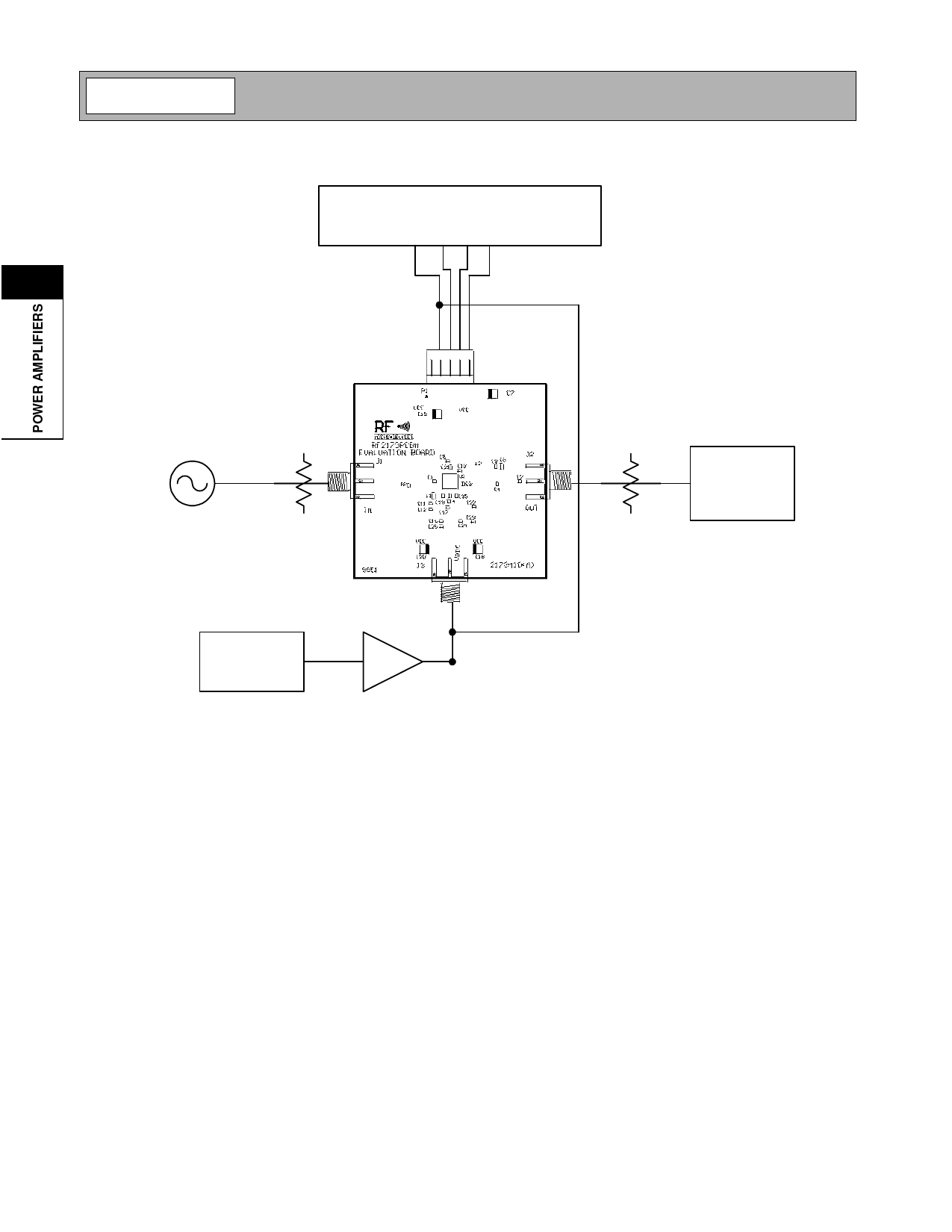
Typical Test Setup
Power Supply
V- V+ S- S+
RF Generator
3dB
Spectrum
Analyzer
10dB/5W
Pulse
Generator
Buffer
x1 OpAmp
A buffer amplifier is recommended because the current into the
VAPC changes with voltage. As an alternative, the voltage may be
monitored with an oscilloscope.
Notes about testing the RF2173
The test setup shown above includes two attenuators. The 3dB pad at the input is to minimize the effects that the
switching of the input impedance of the PA has on the signal generator. When VAPC is switched quickly, the resulting
input impedance change can cause the signal generator to vary its output signal, either in output level or in frequency.
Instead of an attenuator an isolator may also be used. The attenuator at the output is to prevent damage to the spec-
trum analyzer, and should be able to handle the power.
It is important not to exceed the rated supply current and output power. When testing the device at higher than nominal
supply voltage, the VAPC should be adjusted to avoid the output power exceeding +36dBm. During load-pull testing at
the output it is important to monitor the forward power through a directional coupler. The forward power should not
exceed +36dBm, and VAPC needs to be adjusted accordingly. This simulates the behavior for the power control loop in
this respect. To avoid damage, it is recommended to set the power supply to limiting the current during the burst, not to
exceed the maximum current rating.
2-230
Rev A4 010914
Share Link: 