OM7612ST Просмотр технического описания (PDF) - Unspecified
Номер в каталоге
Компоненты Описание
производитель
OM7612ST Datasheet PDF : 4 Pages
| |||
OM7612ST
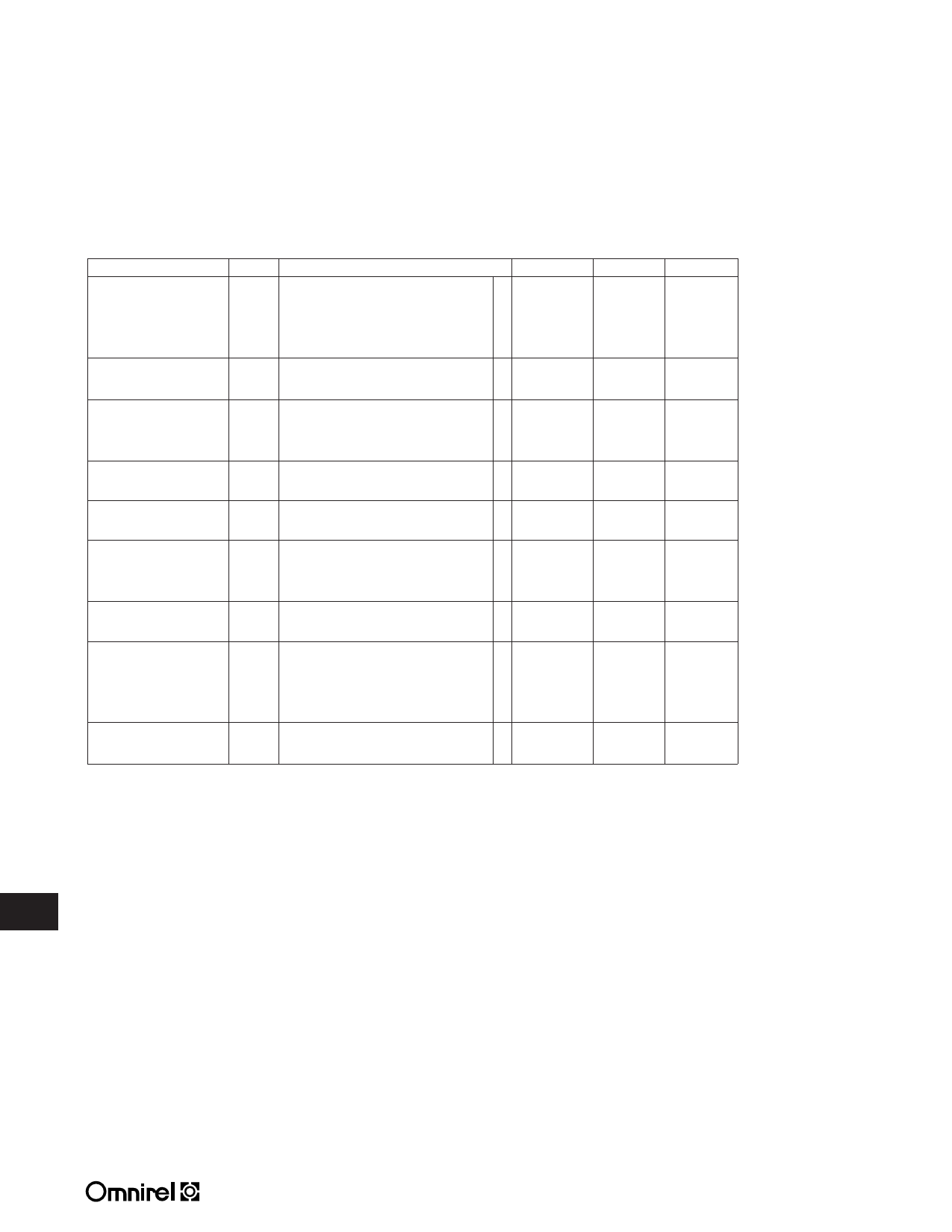
ELECTRICAL CHARACTERISTICS -55°C TA 125°C, IL = 8mA (unless otherwise specified)
Parameter
Symbol
Test Conditions
Min.
Max.
Unit
Reference Voltage
VREF
VDIFF = 3.0V, TA = 25°C
-1.262
-1.238
VDIFF = 3.0V
•
-1.28
-1.22
V
VDIFF = 50V, TA = 25°C
-1.28
-1.22
VDIFF = 50V
•
-1.28
-1.22
Line Regulation
RLINE
3.0 V VDIFF 50V, TA = 25°C
-6
6
(Note 1)
•
-20
20
mV
Load Regulation
RLOAD
VDIFF 50V, 8mA IL 110mA, TA = 25°C
-25
25
(Note 1)
VDIFF = 5V, 8mA IL 1.5A, TA = 25°C
-25
25
mV
•
-50
50
Thermal Regulation
VRTH
Vin = -14.6V, IL = 1.5A
-5
5
mV
Pd = 20 Watts, t = 10 ms, TA = 25°C
Ripple Rejection
RN
f = 120 Hz, VOUT = Vref
•
66
dB
(Note 2)
CAdj = 10 µF, IOUT = 100 mA
Adjustment Pin Current
IAdj
VDIFF = 3.0V
•
100
VDIFF = 40V
•
100
µA
VDIFF = 50V
•
100
Adjustment Pin
³IAdj
VDIFF = 5V, 8mA IOUT 1.5A
•
-5
5
µA
Current Change
3V VDIFF 50V, IL 8mA
•
-6
6
Miminum Load Current
ILmin
VDIFF = 3.0V, VOUT = -1.4V (forced)
•
3
VDIFF = 10V, VOUT = -1.4V (forced)
•
3
mA
VDIFF = 40V, VOUT = -1.4V (forced)
•
5
VDIFF = 50V, VOUT = -1.4V (forced)
•
5
Current Limit
ICL
VDIFF = 5V
•
1.5
3.5
(Note 2)
VDIFF = 50V, TA = 25°C
0.2
1.0
A
Notes:
1. Load and Line Regulation are specified at a constant junction temperature. Pulse testing with low duty cycle is used.
Changes in output voltage due to heating effects must be taken into account separately.
2. If not tested, shall be guaranteed to the specified limits.
3. The • denotes the specifications which apply over the full operating temperature range.
3.3
3.3 - 162
Share Link: 