ICM7231 Просмотр технического описания (PDF) - Intersil
Номер в каталоге
Компоненты Описание
производитель
ICM7231 Datasheet PDF : 16 Pages
| |||
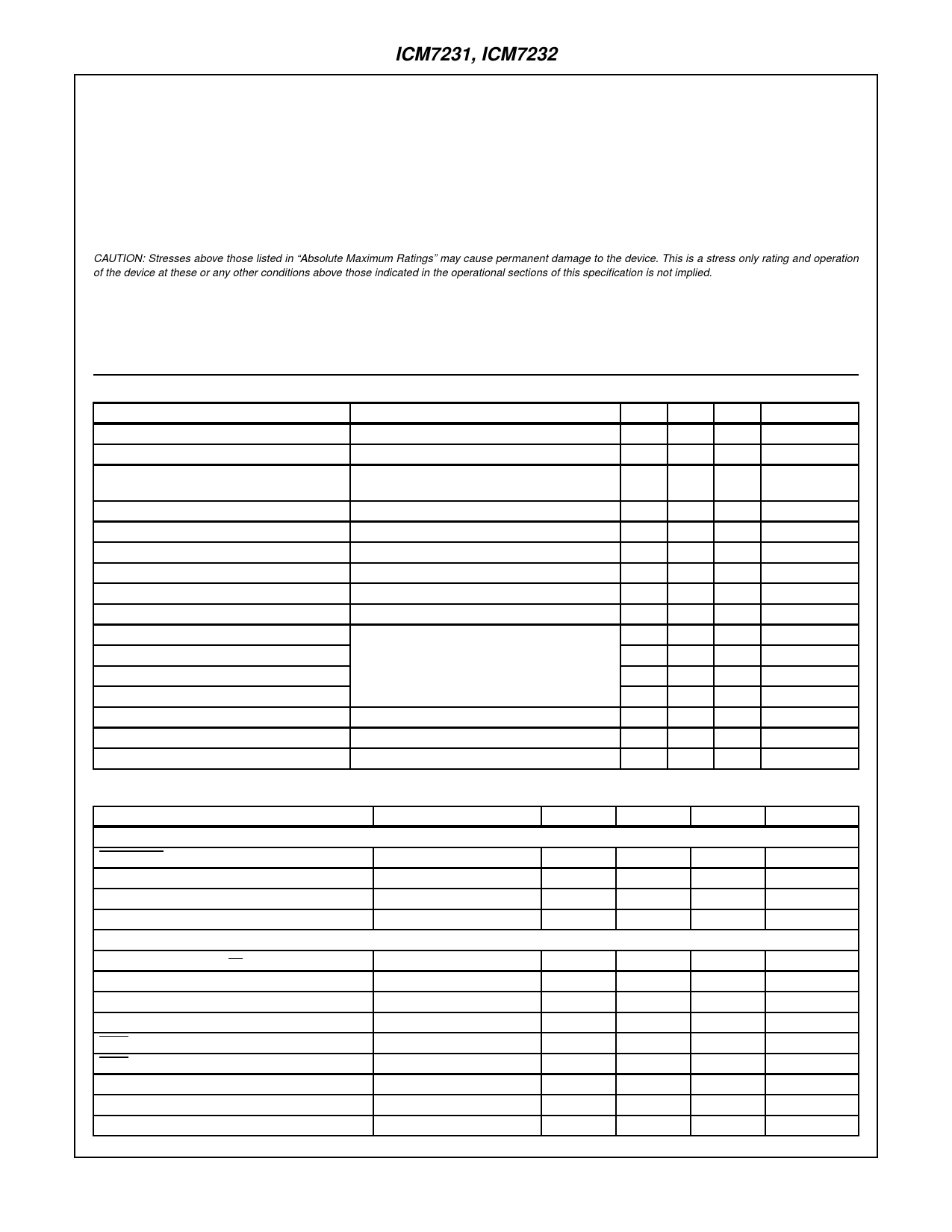
ICM7231, ICM7232
Absolute Maximum Ratings
Supply Voltage (VDD - VSS) . . . . . . . . . . . . . . . . . . . . . . . . . . . . 6.5V
Input Voltage (Note 1). . . . . . . . . . . . . . . . . . . . VSS - 0.3 ≤ VIN ≤ 6.5
Display Voltage (Note 1) . . . . . . . . . . . . . . . . . . . .0.3 ≤ VDISP ≤ +0.3
Operating Conditions
Temperature Range . . . . . . . . . . . . . . . . . . . . . . . . . . -25oC to 85oC
Thermal Information
Thermal Resistance (Typical, Note 2)
θJA (oC/W) θJC (oC/W)
PDIP Package . . . . . . . . . . . . . . . . . . .
60
N/A
CERDIP Package . . . . . . . . . . . . . . . .
50
12
Maximum Junction Temperature
Ceramic Package . . . . . . . . . . . . . . . . . . . . . . . . . . . . . . . . 175oC
Plastic Package . . . . . . . . . . . . . . . . . . . . . . . . . . . . . . . . . . 150oC
Maximum Storage Temperature Range . . . . . . . . . .-65oC to 150oC
Maximum Lead Temperature (Soldering, 10s) . . . . . . . . . . . . 300oC
CAUTION: Stresses above those listed in “Absolute Maximum Ratings” may cause permanent damage to the device. This is a stress only rating and operation
of the device at these or any other conditions above those indicated in the operational sections of this specification is not implied.
NOTES:
1. Due to the SCR structure inherent in these devices, connecting any display terminal or the display voltage terminal to a voltage outside
the power supply to the chip may cause destructive device latchup. The digital inputs should never be connected to a voltage less than
-0.3V below ground, but maybe connected to voltages above VDD but not more than 6.5V above VSS.
2. θJA is measured with the component mounted on an evaluation PC board in free air.
Electrical Specifications V+ = 5V +10%, VSS = 0V, TA = -25oC to 85oC, Unless Otherwise Specified
PARAMETER
TEST CONDITIONS
MIN TYP
Power Supply Voltage, VDD
4.5 >4
Data Retention Supply Voltage, VDD
Guaranteed Retention at 2V
2
1.6
Logic Supply Current, IDD
Current from VDD to Ground Excluding Display. -
30
VDISP = 2V
Shutdown Total Current, IS
VDISP Pin 2 Open
-
1
Display Voltage Range, VDISP
VSS ≤ VDISP ≤ VDD
0
-
Display Voltage Setup Current, IDISP
VDISP = 2V, Current from VDD to VDISP On-Chip -
15
Display Voltage Setup Resistor Value, RDISP One of Three Identical Resistors in String
DC Component of Display Signals
(Sample Test Only)
40
75
-
1/4
Display Frame Rate, fDISP
See Figure 5
60
90
Input Low Level, VIL
Input High Level, VIH
ICM7231, Pins 30 - 35, 37 - 39, 1
ICM7232, Pins 1, 38, 39 (Note 2)
-
-
2.0
-
Input Leakage, IILK
-
0.1
Input Capacitance, CIN
-
5
Output Low Level, VOL
Pin 37, ICM7232, IOL = 1mA
-
-
Output High Level, VOH
VDD = 4.5V, IOH = -500µA
4.1
-
Operating Temperature Range, TOP
Industrial Range
-25
-
MAX
5.5
-
100
UNITS
V
V
µA
10
VDD
30
-
1
120
0.8
-
1
-
0.4
-
+85
µA
V
µA
kΩ
% (VDD - VDISP)
Hz
V
V
µA
pF
V
V
oC
AC Specifications VDD = 5V +10% VSS = 0V, -25oC to 85oC
PARAMETER
TEST CONDITIONS
MIN
TYP
MAX
UNITS
PARALLEL INPUT (ICM7231) See Figure 1
Chip Select Pulse Width, tCS
Address/Data Setup Time, tDS
Address/Data Hold Time, tDH
Inter-Chip Select Time, tICS
SERIAL INPUT (ICM7232) See Figures 2, 3
(Note 1)
(Note 1)
(Note 1)
(Note 1)
500
350
-
ns
200
-
-
ns
0
-20
-
ns
3
-
-
µs
Data Clock Low Time, tCL
Data Clock High Time, tCL
Data Setup Time, tDS
Data Hold Time, tDH
Write Pulse Width, tWP
Write Pulse to Clock at Initialization, tWLL
Data Accepted Low Output Delay, tODL
Data Accepted High Output Delay, tODH
Write Delay After Last Clock, tCWS
(Note 1)
(Note 1)
(Note 1)
(Note 1)
(Note 1)
(Note 1)
(Note 1)
(Note 1)
(Note 1)
350
-
-
ns
350
-
-
ns
200
-
-
ns
0
-20
-
ns
500
350
-
ns
1.5
-
-
µs
-
200
400
ns
-
1.5
3
µs
350
-
-
ns
9-23
Share Link: 