M64897GP(2006) Просмотр технического описания (PDF) - Renesas Electronics
Номер в каталоге
Компоненты Описание
производитель
M64897GP Datasheet PDF : 14 Pages
| |||
M64897GP
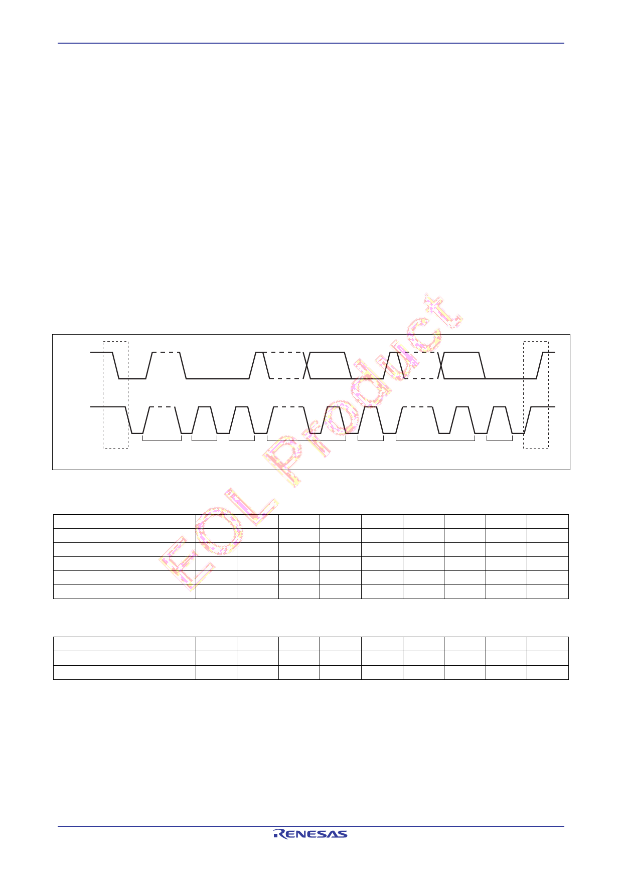
RSa, RSb: Set Up for The Reference Frequency Divider Ratio
RSa
RSb
1
1
0
1
X
0
OS: Set Up The Tuning Amplifier
OS
0
1
Tuning Voltage Output
ON
OFF
POR : Power on reset flag. “1” output at reset
FL : Lock detector flag. “1” output at locked, “0”output at unlocked
A2, A1, A0: 5 Level A/D Converter Output Data
ADC Input Voltage
A2
A1
0.6 ± VCC1 to VCC1
1
0
0.45 ± VCC1 to 0.6 ± VCC1
0
1
0.3 ± VCC1 to 0.45 ± VCC1
0
1
0.15 ± VCC1 to 0.3 ± VCC1
0
0
0 to 0.15 ± VCC1
0
0
Note: The voltage accuracy allowance range: 0.03 ± VCC1 (V)
Divider Ratio
1/512
1/1024
1/640
Mode
Normal
Test
A0
0
1
0
1
0
Power on Reset Operation
(Initial state the power is turned ON)
BS4 to BS1
: OFF
Charge pump
: High impedance
Tuning amplifier
: OFF
Charge pump current : 270 µA
Frequency division ratio : 1/1024
Lock detect
:H
Charge pump current is replaced by 70 µA when locks it by automatic change facility.
Rev.2.00 Jun 14, 2006 page 10 of 13
Share Link: 