M64894 Просмотр технического описания (PDF) - MITSUBISHI ELECTRIC
Номер в каталоге
Компоненты Описание
производитель
M64894 Datasheet PDF : 8 Pages
| |||
MITSUBISHI ICS (TV)
M64894FP/GP
SERIAL INPUT PLL FREQUENCY SYNTHESIZER FOR TV/VCR
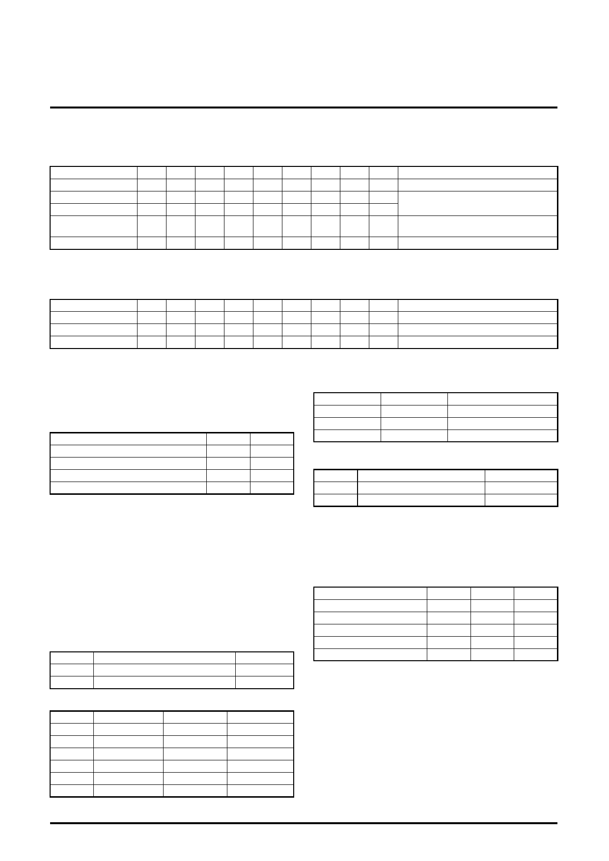
DATA CORDING EXAMPLE
Write mode format example
Byte
Address Byte
Devider Byte1
Devider Byte2
Control Byte1
Band SW Byte
MSB
LSB
Condotion in data setting
1
1
0
0
0
1
1
0
1 ADS input VCC1
0
1
0
0
0
0
0
0
1
Dividing ratio N=16544
1
0
1
0
0
0
0
0
1
1
1
0
0
0
0
1
0
1
C.P. current 270µA
fREF division ratio 1/1024
0
0
0
0
1
0
0
0
1 BS4 output ON
fVCO=N×8×fREF=16544×8×(4MHz/1024)=517MHz
Read mode format example
Byte
MSB
LSB
Condotion in divise
Address Byte
1
1
0
0
0
1
1
1
1
Status Byte1 input
1
1
1
1
1
1
1
1
1
Status Byte1 output
0
1
1
1
1
0
1
1
1 FL “1”output at locked ADC input at open
TEST MODE DATA SET UP METHOD
Test Mode Bit Set Up
X
: Random, 0 or 1. normal "0"
MA1 ,MA0 : Programmabule Address Bit
Address input voltage
0 to 0.1∗VCC1
Always valid
0.4∗VCC1 to 0.6*VCC1
0.9∗VCC1 to VCC1
MA1
0
0
1
1
MA0
0
1
0
1
N14 to N0 : How to set dividing ratio of the programable the divider
Dividing ratio N=N14(214=16384)+ ⋅⋅⋅ +N0(20=1)
Therefore, the range of division N is 1,024 to 32,768
Example) fvco=fREF×8×N
=3.90625×8×N
=31.25×N (kHz)
CP: Setting up the charge pump current of the phase
comparator
CP
Charge pump current
Mode
0
70µA
Test
1
270µA
Normal
T2, T1, T0 : Setting up for the test mode
T2 T1 T0
00X
01X
110
111
100
101
Charge pump
Normal operation
High impedance
Sink
Source
High impedance
High impedance
Pin 12 condition
Mode
ADC input
Normal operation
ADC input
Test mode
ADC input
Test mode
ADC input
Test mode
fREF output
Test mode
f1/N output
Test mode
RSa, RSb : Set up for the reference frequency division ratio
RSa
RSb
1
1
0
1
X
0
Division ratio
1/512
1/1024
1/640
OS : Set up the tuning amplifier
OS
Tuning voltage output
0
ON
1
OFF
POR
FL
: Power on reset flag. “1” output at reset
: Lock detecter flag. “1” output at locked,
“0” output at unlocked
Mode
Normal
Test
A2, A1, A0: 5level A/D converter output data
ADC input voltage
0.6∗VCC1 to VCC1
0.45∗VCC1 to 0.6∗VCC1
0.3∗VCC1 to 0.45∗VCC1
0.15∗VCC1 to 0.3∗VCC1
0 to 0.15∗VCC1
A2
A1
A0
1
0
0
0
1
1
0
1
0
0
0
1
0
0
0
The voltage accuracy allowance range: ±0.03∗VCC1 (V)
POWER ON RESET OPERATION
(Initial state the power is turned ON)
BS4 to BS1
: OFF
Charge pump
: High impedance
Tuning amplifier
: OFF
Charge pump current : 270µA
Frequency division ratio : 1/1024
6
Share Link: 