M64811AGP Просмотр технического описания (PDF) - MITSUBISHI ELECTRIC
Номер в каталоге
Компоненты Описание
производитель
M64811AGP Datasheet PDF : 9 Pages
| |||
MITSUBISHI ICs (COMMUNICATION)
M64811AGP
1.1GHz/500MHz DUAL PLL FREQUENCY SYNTHESIZER FOR DIGITAL CELLULAR PHONE
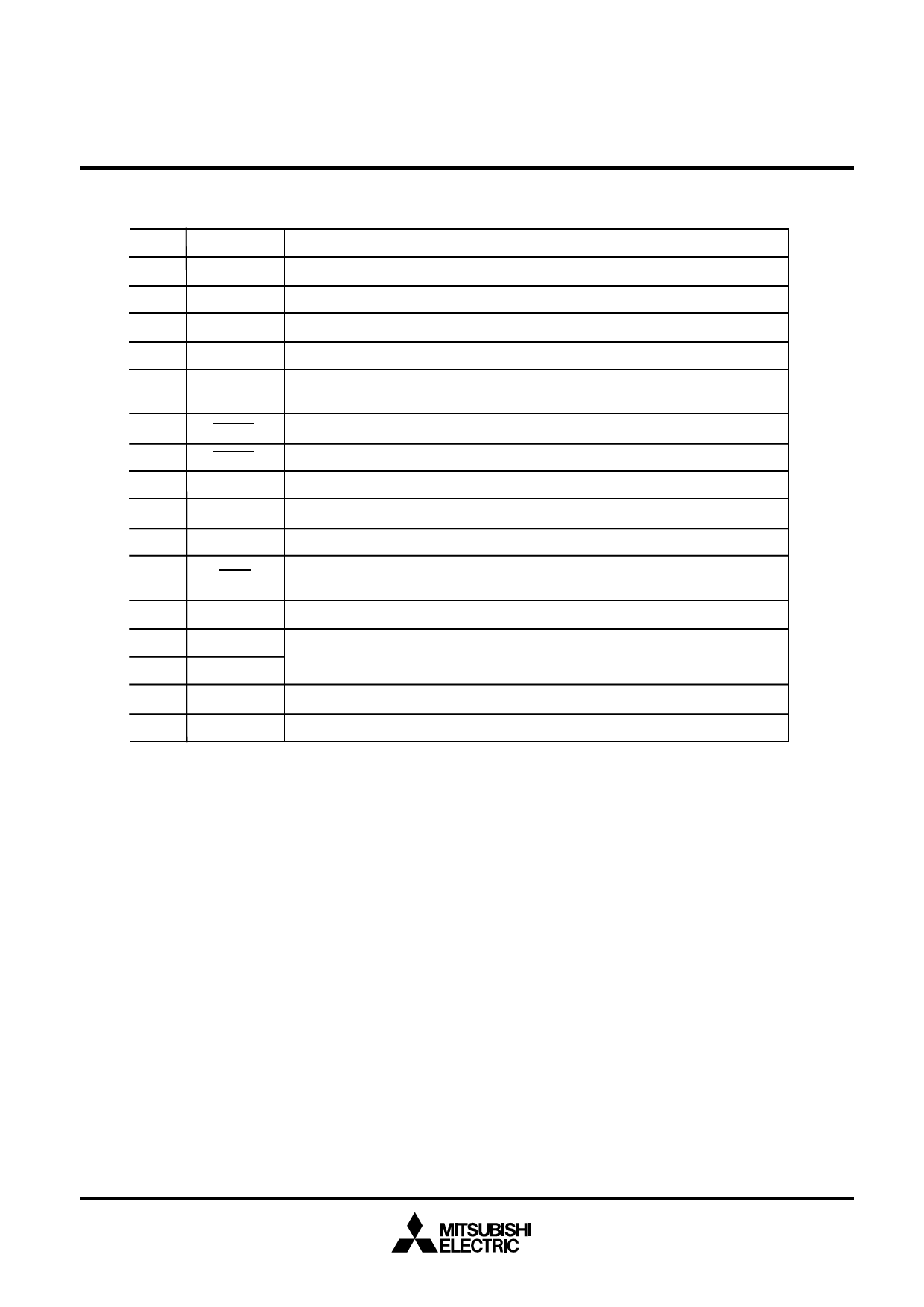
FUNCTION DESCRIPTION OF PINS
Pin No. Pin Identification
Description
1
FIN1
Input from the VCO , Fmax = 1.1GHz .
2
GND
Ground .
3
CPS
Clock pulse input . Shift register clock input pin .
4
SI
Binary serial data input . Shift register data input pin
Load enable input . When LE is HIGH , data stored in the shift registers is loaded into the
5
LE
appropriate latch .
6
SLEEP1
PLL1 power control . "H" = normal operation , "L"=power down .
7
SLEEP2
PLL2 power control . "H" = normal operation , "L"=power down .
8
FIN2
Input from the VCO , Fmax = 500MHz .
9
PD2
Charge pump2 output . Tristate output . High Z when PLL2 power is off .
10
GND
Ground .
11
LOCK
When loops are locked ••••••••"L" , When one of loops is unlocked••••••••"High Z" .
If one loop is sleep mode , the status of the other loop is checked for judgment .
12
XBo
Buffer output of oscillator .
13
XOUT
Crystal Oscillator input .
14
XIN
15
Vcc
Power supply . Vcc = 2.7~3.6V .
16
PD1
Charge pump1 output . Tristate output . High Z when PLL1 power is off .
3
Share Link: 