M62501FP Просмотр технического описания (PDF) - Renesas Electronics
Номер в каталоге
Компоненты Описание
производитель
M62501FP Datasheet PDF : 11 Pages
| |||
M62501P/FP
Terminal
No.
6
7
8
Symbol
P.OUT
OVP
UVP
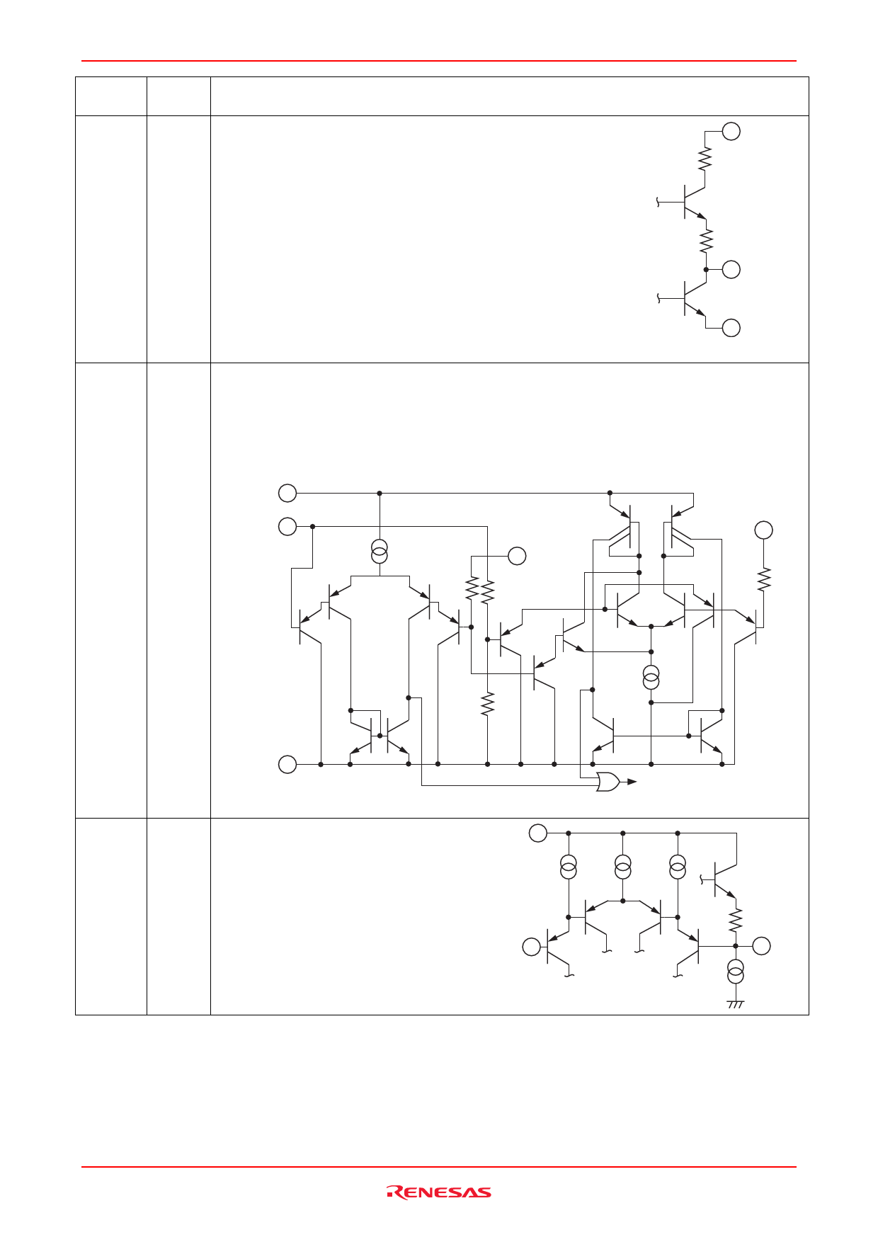
Function and Terminal Circumscription Circuitry
The abnormal state detection output terminal
• The output becomes "H" from "L" when an abnormality is detected
in the OVP or UVP terminal. Then the PWM output terminal
becomes "H" settlement, too.
• Do OFF of power supply (VCC) to remove latch of abnormal state.
• In abnormal state detection;
Output "H" level = 10.5 V typ
(The output load current: no-load, VCC = 12 V)
Output "L" level = 1.5 V typ
(The output load current: −1 mA, VCC = 12 V)
• In normal state ;
Output "L" level = 0.4 V typ
(The output load current: +10 mA, VCC = 12 V)
Over voltage protection of the control line (OVP)
• Setting terminal voltage;
GND ≤ VOVP < VREF
Under voltage protection of the control line (UVP)
• Setting terminal voltage;
GND ≤ VUVP < VOVP
VCC 2
VREF 15
OVP
7
2 VCC
6 P. OUT
16 GND
UVP
8
9
BI
10
BO
GND 16
To latch Input
Note: lt is connected to GND when the abnormal detection terminal is not used.
The input terminal of a buffer Amp. (BI)
The output terminal of a buffer Amp. (BO)
VCC 2
BI 9
10 BO
Rev.2.00 Jun 14, 2006 page 5 of 10
Share Link: 