LT5504 Просмотр технического описания (PDF) - Linear Technology
Номер в каталоге
Компоненты Описание
производитель
LT5504 Datasheet PDF : 8 Pages
| |||
LT5504
PI FU CTIO S
VCC (Pins 1, 8 ): Power Supply Pins. These pins must be
tied together at the part as close as possible, and should
be decoupled using 1000pF capacitors.
RF+ (Pin 2): Positive RF Input Pin.
RF– (Pin 3): Negative RF Input Pin.
GND (Pin 4): Ground Pin.
EN (Pin 5): Enable Pin. The on/off threshold voltage
is about VCC/2. When the input voltage is higher than
0.6 • VCC, the circuit is completely turned on. When the
input voltage is less than 0.4 • VCC, the circuit is turned off.
LO (Pin 6): Local Oscillator Input Pin.
VOUT (Pin 7): Output Pin.
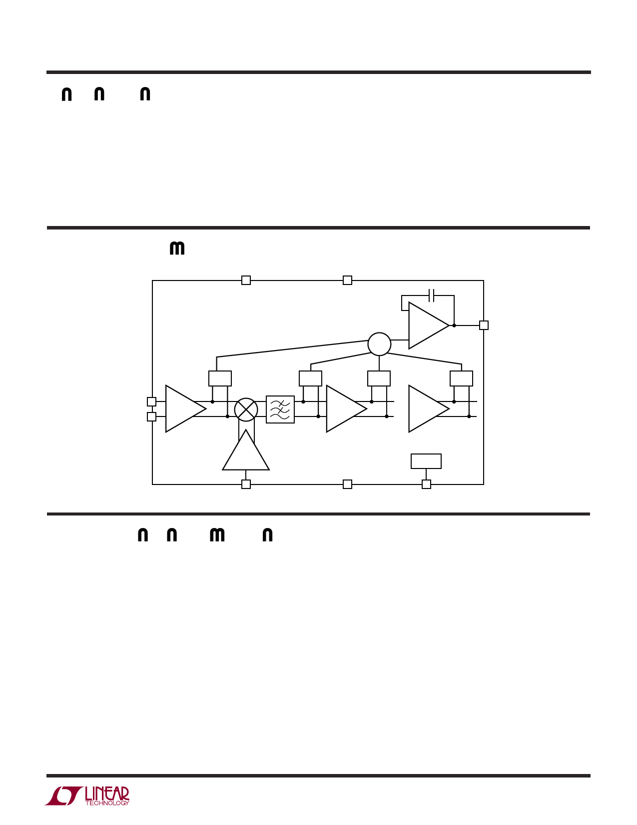
BLOCK DIAGRA
VCC
VCC
1
8
7 VOUT
+
RF+ 2
RF– 3
RF
LIMITER
DET
DET
DET
DET
LIMITING
MIXER
LPF
IF
LIMITER
IF
• • • LIMITER
LO
BUFFER
6
LO
4
GND
ENABLE
5
EN
5504 BD
APPLICATIO S I FOR ATIO
The LT5504 consists of the following sections: RF/IF
limiters, limiting mixer, RF/IF detectors, LO buffer ampli-
fier, 3rd-order integrated low pass filter (LPF), output
interface and bias circuitry.
An RF signal ranging from 800MHz to 2.7GHz is detected
by the RF and IF detectors using a proprietary technique.
The down-converted IF signal is band limited by the on-
chip LPF, reducing broadband noise, and thus an ultrawide
dynamic range signal can be measured. The RF measuring
receiver is essentially a logarithmic voltage detector. The
measured output voltage is directly proportional to the RF
signal voltage. An internal temperature compensation
circuit results in a highly temperature-stable output volt-
age.
RF Limiter
The differential input impedance of the RF limiter is shown
in Figure 1. A 1:1 input transformer can be used to achieve
50Ω broadband matching with an 82Ω shunt resistor (R1)
at the inputs as shown in Figure 5.
The 1:1 RF input transformer can also be replaced with a
narrow band single-ended-to-differential conversion cir-
cuit using three discrete elements as shown in Figure 2.
Their nominal values are listed in Table 1. Due to the
parasitics of the PCB, these values may require adjust-
ment.
5504f
5
Share Link: 